
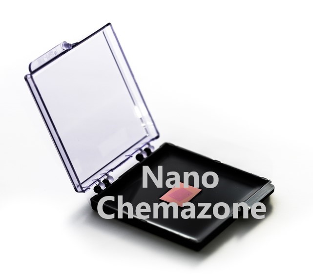


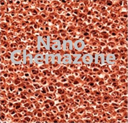

CVD Graphene on Copper Foil
₹0.00
CAS No.: 7782-42-5 (graphene), 7440-50-8 (copper)
PREPARATION METHOD: CVD Method
WAFER STRUCTURE: Graphene on Copper Foil (both sides), Copper Foil 45 µm
CHARACTERIZATION & ANALYSIS
Predominantly Single-layer Graphene on Copper Substrate
| Sheet Resistance | <600Ω/sq |
| Custom Order | <300Ω/sq |
| Transparency | >95% |
| Product Name |
CVD Graphene on Copper Foil |
| Stock No. | NCZ-GSW-0016 |
| Purity | > 99.9% |
| Graphene Film | |
| FET Electron Mobility on Al2O3 | 2000 cm2/Vs |
| Hall Electron Mobility on SiO2/Si | 4000 cm2/Vs |
Description
Note: For pricing & ordering information, please contact us at sales@nanochemazone.com
Please contact us for quotes on Larger Quantities & Customization. E-mail: contact@nanochemazone.com
Customization:
If you are planning to order large quantities for your industrial and academic needs, please note that customization of parameters (such as size, length, purity, functionalities, etc.) are available upon request.
Shipping & Delivery
Related products

CVD Graphene on Silicon Substrate
| Product Name |
CVD Graphene On Silicon Substrate |
| Stock No. | NCZ-GSW-0017 |
| Purity | > 99.9% |
| Graphene Film | |
| FET Electron Mobility on Al2O3 | 2000 cm2/Vs |
| Hall Electron Mobility on SiO2/Si | 4000 cm2/Vs |
| Sheet Resistance | 450±40 Ω/sq (1cm x1cm) |
| Transparency | >95% |
- Copper-based graphene is prepared by CVD method.
- Graphene is transferred from copper to silicon substrate.
SILICON WAFER:
| Wafer Thickness: | 525 µm, (customization is possible) |
| Resistivity: | <0.01 ohm-cm |
| Type/Dopant: | P/N |
| Orientation: | <100> (customization is possible) |
| Front Surface: | Polished |
| Back Surface: | Etched |
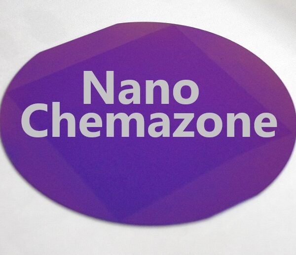
CVD Graphene on SiO2 Substrate
| Product Name |
CVD Graphene on SiO2 Substrate/Wafer |
| Stock No. | NCZ-GSW-0018 |
| Purity | > 99.9% |
| Graphene Film | |
| FET Electron Mobility on Al2O3 | 2000 cm2/Vs |
| Hall Electron Mobility on SiO2/Si | 4000 cm2/Vs |
| Sheet Resistance | <600Ω/sq |
| Custom Order | <300Ω/sq |
| Transparency | >95% |
| CVD Graphene | Substrate |
| 1cm x 1cm | 1.5cm x 1.5cm, thickness: 300nm SiO2/700um Si |
| 1inch x 1inch | 3.0cm x 3.0cm, thickness: 300nm SiO2/700um Si |
| 3cm x 3cm | 3.5cm x 3.5cm, thickness: 300nm SiO2/700um Si |
| 7cm x 7cm | Diameter: 4inch, thickness: 300nm SiO2/600um Si |

Graphene & Carbon Nanotubes Water Paste
| MF | C |
| Chemical Name |
Graphene and Carbon Nanotubes Dispersion Mixture |
| Purity | ≥99.5% |
| Diameter | Graphene 5-7 μm, CNT Outside Diameter: 50-80 nm, Inside Diameter: 5-15 nm (Customization possible) |
| Length | 10-20 μm (Customization possible) |
| Number of Layers | <30 (Customization possible) |
| Color | Black |
| Form | Dispersion/Paste/Solution |
| Product Number | NCZC1010 |
| CAS Number | 7782-42-5 |

Graphene Nanoplatelets Powder
Graphene Nanoplatelets Powder (> 99.5 wt%, D 5-10 um, < 20 layers)
Please contact us for customization and price inquiry.
Graphene Nanoplatelets Powder
| MF | C |
| Chemical Name |
Graphene Nanoplatelets |
| Purity | ≥99.5% |
| Diameter | 5-10 µm |
| Thickness | 4-20 nm |
| Number of Layers | <30 (Customization possible) |
| Color | Black |
| Form | Dispersion/Paste/Solution/Powder |
| Product Number | NCZC1007 |
| CAS Number | 7782-42-5 |

Graphene on Silicon Nitride TEM Grids
Graphene on Silicon Nitride TEM Grids
| Product Name | Graphene on Silicon Nitride TEM Grids |
| Stock No. | NCZ-GSW-0012 |
| Purity | > 99.9% |
| Graphene Film | |
| FET Electron Mobility on Al2O3 | 2000 cm2/Vs |
| Hall Electron Mobility on SiO2/Si | 4000 cm2/Vs |
| Sheet Resistance | 450±40 Ω/sq (1cm x1cm) |
- Four thicknesses of CVD graphene: Available in either 1, 2, 3-5 or 6-8 layers
- TEM Substrate: 200 µm thick 3.0mm hexagonal silicon substrate with a 0.5x0.5mm aperture and 200nm thick silicon nitride membrane with approximately 6,400 2.5µm holes
- Graphene coverage of the TEM grid is > 75%
| Type | Thickness of the Graphene | Transparency | TEM Grid/AFM Substrate | Support Film |
| 1 Layer | ~ 0.35 nm | ~ 96.4% | 2.5 μm Hole Silicon Nitride | Silicon Nitride |
| 2 Layers | ~0.7 nm | ~92.7% | 2.5 μm Hole Silicon Nitride | Silicon Nitride |
| 3-5 Layers | 1.0-1.7 nm | ~85.8-90.4% | 2.5 μm Hole Silicon Nitride | Silicon Nitride |
| 6-8 Layers | 2.1-2.8 nm | ~78.5-83.2% | 2.5 μm Hole Silicon Nitride | Silicon Nitride |

Graphene on SiO2 Substrate
Graphene on Ultra-Flat Thermal SiO2 Substrate
| Product Name | Graphene on Ultra-Flat Thermal SiO2 Substrate |
| Stock No. | NCZ-GSW-0011 |
| Purity | > 99.9% |
| Graphene Film | |
| FET Electron Mobility on Al2O3 | 2000 cm2/Vs |
| Hall Electron Mobility on SiO2/Si | 4000 cm2/Vs |
| Sheet Resistance | 450±40 Ω/sq (1cm x1cm) |
- Four thicknesses of CVD graphene: Available in either 1, 2, 3-5 or 6-8 layers
- The Ultra-flat Thermal SiO2 Substrate consists of a 200 nm thermally grown SiO2 film on an ultra-flat silicon wafer with a normal thickness of 675 µm. The size is 5mm x 5mm.
- Graphene coverage of the TEM grid is 75-95 %
| Type | Thickness of the Graphene | Transparency | Support Film |
| 1 Layer | ~0.35nm | ~96.4% | Ultra-flat Silicon |
| 2 Layers | ~0.7nm | ~92.7% | Ultra-flat Silicon |
| 3-5 Layers | 1.0-1.7nm | ~85.8-90.4% | Ultra-flat Silicon |
| 6-8 Layers | 2.1-2.8nm | ~78.5-83.2% | Ultra-flat Silicon |

Hydroxylated Graphene Quantum Dots
Hydroxylated Graphene Quantum Dots
| CAS Number | 7440-40-0 |
| Product Number | NCZC3002 |
| Concentration | 1mg/mL to 20 mg/mL (in stock), Concentration Customization is Possible |
| Carrier | Water, Ethanol, IPA, NMP, Toluene, Methanol, Dispersion Customization is Possible |
| APS | 5-10 nm (Customization is Possible) |
| Package Size | 1-100 mL (Customization is Possible) |
| Composition: | Hydroxylated Graphene Quantum Dots |
| Appearance: | Colorless solution |
| PL peak: | 480 nm (reference only, the actual value may vary) |
| Particle Size: | <10 nm |
| Concentration: | 1 mg/ml (available up to 20mg/ml) |
| Solution: | Water, a mixture of water and ethylene glycol (customization possible) |
| Purity: | > 99.9% |
