Product Name: Single crystal silicon wafer Intrinsic (2-inch)
Product Name
Single crystal silicon wafer Intrinsic (2-inch)
Cat No.
NCZ-NSC329/20
Diameter
2 inch
Doping
Intrinsic
Resistivity
(>1000ohm/sq.)
Thickness
400µm
Orientation
100
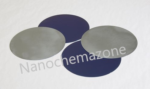
Polished
Single side polished
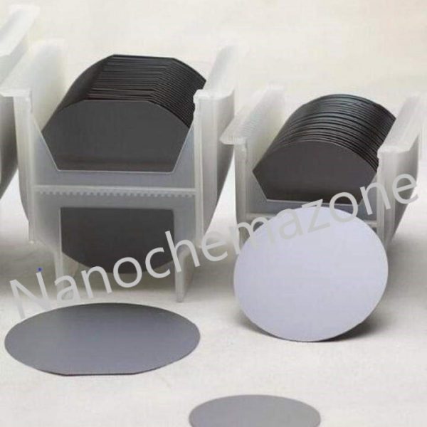
Provided in a Single wafer case:
Description:
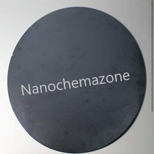
Single crystal silicon wafer Intrinsic (2-inch) is the most widely used semiconductor material as a substrate material due to its excellent machinability, mechanical stability, and the potential to combine sensing elements and electronics on the same substrate. Circular wafers made of silicon are used as a substrate in most MEMS sensors.
The crystal orientation should be known before manufacturing since silicon has orientation-dependent properties such as piezoresistivity coefficients and etching rates. The common orientation is (100) where the numbers represent Miller indices.
As an example, (100) wafer that has a primary flat side as an indication of < 110 > direction. When a piezoresistive element is placed on a (100) wafer, the orientation should be parallel to < 110 > direction if the piezoresistivity coefficients in that direction are intended to be utilized.
If you are planning to order large quantities for your industrial and academic needs, please note that customization of parameters (such as size, length, purity, functionalities, etc.) are available upon request.
Reviews
There are no reviews yet.
Be the first to review “Single crystal silicon wafer Intrinsic (2-inch)” Cancel reply
 1")

Reviews
There are no reviews yet.