
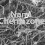
Graphene on Ultra-Fine 200 Mesh Copper TEM Grids
₹0.00
Graphene coated TEM Grids
| Product Name | Graphene On Ultra-Fine 200 Mesh Copper TEM Grids |
| Stock No. | NCZ-GSW-0014 |
| Purity | > 99.9% |
| Graphene Film | |
| FET Electron Mobility on Al2O3 | 2000 cm2/Vs |
| Hall Electron Mobility on SiO2/Si | 4000 cm2/Vs |
| Sheet Resistance | 450±40 Ω/sq (1cm x1cm) |
CAS No.: 7782-42-5
Characteristics
- Four thicknesses of CVD graphene: Available in either 1, 2, 3-5 or 6-8 layers
- TEM Substrate: Microporous Copper TEM Grids with Beryllium-Copper Support Aperture
- Graphene coverage of the TEM grid is better than 75%
Appearance
The graphene film appears as a near-transparent to light-grey film on the surface of the red-brown microporous copper TEM grid. For support, the TEM grid is attached using epoxy to a gold-colored beryllium-copper disk with a 2x1mm aperture.
| Type | Thickness of the Graphene | Transparency | TEM Grid/AFM Substrate | Support Film |
| 1 Layer | ~0.35 nm | ~96.4% | 200 Mesh Copper Grid | N/A |
| 2 Layers | ~0.7 nm | ~92.7% | 200 Mesh Copper Grid | N/A |
| 3-5 Layers | 1.0-1.7 nm | ~85.8-90.4% | 200 Mesh Copper Grid | N/A |
| 6-8 Layers | 2.1-2.8 nm | ~78.5-83.2% | 200 Mesh Copper Grid | N/A |
Please contact us for customization and price inquiry.
Note: For pricing & ordering information, please contact us at sales@nanochemazone.com
Please contact us for quotes on Larger Quantities & Customization. E-mail: contact@nanochemazone.com
Customization:
If you are planning to order large quantities for your industrial and academic needs, please note that customization of parameters (such as size, length, purity, functionalities, etc.) are available upon request.
Related products
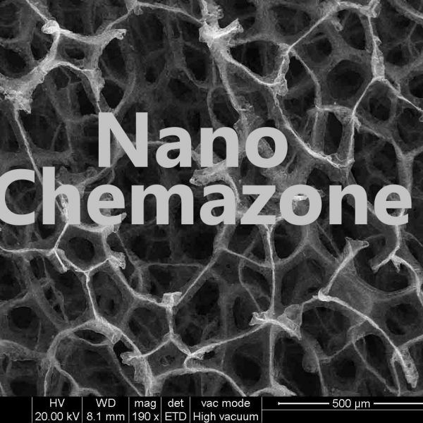
3D Freestanding Graphene Foam
| Product Name |
3D Freestanding Graphene Foam |
| Stock No. | NCZ-GSW-0023 |
| Purity | > 99.9% |
| Graphene Film | |
| FET Electron Mobility on Al2O3 | 2000 cm2/Vs |
| Hall Electron Mobility on SiO2/Si | 4000 cm2/Vs |
PRODUCT DETAIL
CAS No.: 7440-44-0
Density: ~ 0.2g/cm3
Thickness: ~ 0.5mm
Number of layers: ~ 8 layers
| Sheet Resistance | <600Ω/sq |
| Custom Order | <300Ω/sq |
| Transparency | >95% |
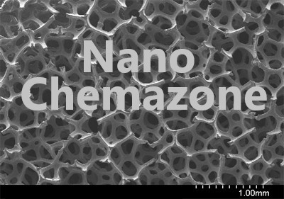
3D Graphene on Nickel/Copper Foam
CAS No.: 7782-42-5 (graphene), 7440-02-0 (nickel)
| Sheet Resistance | <600Ω/sq |
| Custom Order | <300Ω/sq |
| Transparency | >95% |
| Product Name |
3D Graphene on Nickel/Copper Foam |
| Stock No. | NCZ-GSW-0022 |
| Purity | > 99.9% |
| Graphene Film | |
| FET Electron Mobility on Al2O3 | 2000 cm2/Vs |
| Hall Electron Mobility on SiO2/Si | 4000 cm2/Vs |

CVD Graphene on PET Substrate
| Product Name |
CVD Graphene on PET Substrate |
| Stock No. | NCZ-GSW-0019 |
| Purity | > 99.9% |
| Graphene Film | |
| FET Electron Mobility on Al2O3 | 2000 cm2/Vs |
| Hall Electron Mobility on SiO2/Si | 4000 cm2/Vs |
PRODUCT DETAIL
CAS No.: 7782-42-5 (graphene), 25038-59-9 (PET)
PET Substrate: ~188µm thick
| Sheet Resistance | <600Ω/sq |
| Custom Order | <300Ω/sq |
| Transparency | >95% |

CVD Graphene on Quartz Substrate
| Product Name |
CVD Graphene on Quartz Substrate |
| Stock No. | NCZ-GSW-0020 |
| Purity | > 99.9% |
| Graphene Film | |
| FET Electron Mobility on Al2O3 | 2000 cm2/Vs |
| Hall Electron Mobility on SiO2/Si | 4000 cm2/Vs |
PRODUCT DETAIL
CAS No.: 7782-42-5 (graphene)
| Sheet Resistance | <600Ω/sq |
| Custom Order | <300Ω/sq |
| Transparency | >95% |
| CVD Graphene | Substrate |
| 1cm x 1cm | Diameter: 1inch, Thickness: 3mm* |
| 1inch x 1inch | 30mm x 30mm, Thickness: 1mm |
We can also provide 15mm x 15mm and 1mm thick substrate and other sizes based on your request. Please contact us for more information.
CVD Graphene on SiO2 Substrate
| Product Name |
CVD Graphene on SiO2 Substrate/Wafer |
| Stock No. | NCZ-GSW-0018 |
| Purity | > 99.9% |
| Graphene Film | |
| FET Electron Mobility on Al2O3 | 2000 cm2/Vs |
| Hall Electron Mobility on SiO2/Si | 4000 cm2/Vs |
PRODUCT DETAIL
CAS No.: 7782-42-5 (graphene), 7631-86-9 (silicon dioxide), 7440-21-3 (silicon)
| Sheet Resistance | <600Ω/sq |
| Custom Order | <300Ω/sq |
| Transparency | >95% |
GRAPHENE ON SILICON DIOXIDE (300NM)/SI SUBSTRATE (P-TYPE, 1-10 Ω·CM)
| CVD Graphene | Substrate |
| 1cm x 1cm | 1.5cm x 1.5cm, thickness: 300nm SiO2/700um Si |
| 1inch x 1inch | 3.0cm x 3.0cm, thickness: 300nm SiO2/700um Si |
| 3cm x 3cm | 3.5cm x 3.5cm, thickness: 300nm SiO2/700um Si |
| 7cm x 7cm | Diameter: 4inch, thickness: 300nm SiO2/600um Si |

Graphene on Lacey Carbon 300 Mesh Copper TEM Grids
Graphene On Lacey Carbon 300 Mesh Copper TEM Grids
| Product Name | Graphene On Lacey Carbon 300 Mesh Copper TEM Grids |
| Stock No. | NCZ-GSW-0015 |
| Purity | > 99.9% |
| Graphene Film | |
| FET Electron Mobility on Al2O3 | 2000 cm2/Vs |
| Hall Electron Mobility on SiO2/Si | 4000 cm2/Vs |
| Sheet Resistance | 450±40 Ω/sq (1cm x1cm) |
PRODUCT DETAIL
CAS No.: 7782-42-5
Graphene TEM Support Films are supported by a lacey carbon film on a 300 mesh copper TEM grid.
Characteristics
- Four thicknesses of CVD graphene: Available in either 1, 2, 3-5 or 6-8 layers
- TEM Substrate: Lacey carbon support film on 300 mesh copper TEM grid
- Graphene coverage of the TEM grid is better than 75%
Appearance
The graphene film appears as a near-transparent to light-grey film on the surface of the Lacey Carbon mesh on a red-brown colored copper TEM grid.
| Type | Thickness of the Graphene | Transparency | TEM Grid/AFM Substrate | Support Film |
| 1 Layer | ~0.35 nm | ~96.4% | 300 Mesh Copper Grid | N/A |
| 2 Layers | ~0.7 nm | ~92.7% | 300 Mesh Copper Grid | N/A |
| 3-5 Layers | 1.0-1.7 nm | ~85.8-90.4% | 300 Mesh Copper Grid | N/A |
| 6-8 Layers | 2.1-2.8 nm | ~78.5-83.2% | 300 Mesh Copper Grid | N/A |
Please contact us for customization and price inquiry.

Graphene on Silicon Nitride TEM Grids
Graphene on Silicon Nitride TEM Grids
| Product Name | Graphene on Silicon Nitride TEM Grids |
| Stock No. | NCZ-GSW-0012 |
| Purity | > 99.9% |
| Graphene Film | |
| FET Electron Mobility on Al2O3 | 2000 cm2/Vs |
| Hall Electron Mobility on SiO2/Si | 4000 cm2/Vs |
| Sheet Resistance | 450±40 Ω/sq (1cm x1cm) |
PRODUCT DETAIL
Characteristics
- Four thicknesses of CVD graphene: Available in either 1, 2, 3-5 or 6-8 layers
- TEM Substrate: 200 µm thick 3.0mm hexagonal silicon substrate with a 0.5x0.5mm aperture and 200nm thick silicon nitride membrane with approximately 6,400 2.5µm holes
- Graphene coverage of the TEM grid is > 75%
Appearance
Solid hexagonal disk with a greenish hue. The graphene film appears as a near-transparent to light-grey film on the surface of the microporous silicon Nitride membrane.
| Type | Thickness of the Graphene | Transparency | TEM Grid/AFM Substrate | Support Film |
| 1 Layer | ~ 0.35 nm | ~ 96.4% | 2.5 μm Hole Silicon Nitride | Silicon Nitride |
| 2 Layers | ~0.7 nm | ~92.7% | 2.5 μm Hole Silicon Nitride | Silicon Nitride |
| 3-5 Layers | 1.0-1.7 nm | ~85.8-90.4% | 2.5 μm Hole Silicon Nitride | Silicon Nitride |
| 6-8 Layers | 2.1-2.8 nm | ~78.5-83.2% | 2.5 μm Hole Silicon Nitride | Silicon Nitride |
Please contact us for customization and price inquiry.

Graphene on SiO2 Substrate
Graphene on Ultra-Flat Thermal SiO2 Substrate
| Product Name | Graphene on Ultra-Flat Thermal SiO2 Substrate |
| Stock No. | NCZ-GSW-0011 |
| Purity | > 99.9% |
| Graphene Film | |
| FET Electron Mobility on Al2O3 | 2000 cm2/Vs |
| Hall Electron Mobility on SiO2/Si | 4000 cm2/Vs |
| Sheet Resistance | 450±40 Ω/sq (1cm x1cm) |
PRODUCT DETAIL
Characteristics
- Four thicknesses of CVD graphene: Available in either 1, 2, 3-5 or 6-8 layers
- The Ultra-flat Thermal SiO2 Substrate consists of a 200 nm thermally grown SiO2 film on an ultra-flat silicon wafer with a normal thickness of 675 µm. The size is 5mm x 5mm.
- Graphene coverage of the TEM grid is 75-95 %
| Type | Thickness of the Graphene | Transparency | Support Film |
| 1 Layer | ~0.35nm | ~96.4% | Ultra-flat Silicon |
| 2 Layers | ~0.7nm | ~92.7% | Ultra-flat Silicon |
| 3-5 Layers | 1.0-1.7nm | ~85.8-90.4% | Ultra-flat Silicon |
| 6-8 Layers | 2.1-2.8nm | ~78.5-83.2% | Ultra-flat Silicon |
Please contact us for customization and price inquiry.