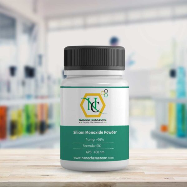
Silicon Monoxide (SiO)
Product Name: Silicon Monoxide Powder
| Product Name |
Silicon Monoxide |
| Cat No. |
NCZ-MN-056/20 |
| CAS No. |
10097-28-6 |
| MF |
SiO |
| Purity |
>99% |
| APS |
400 nm (Customizable) |
| Appearance |
Black Brown Powder |
| Molecular Weight |
44.08 |
| Melting Point |
1702°C |
| Boiling Point |
1880°C |
| Density |
2.13g/cm³ |
| Refractive index |
1.980 |
| Application |
Plating of optical equipment such as lens |
| Crushing to submicron level below D50 |
500 nm is also available |
Silicon Monoxide Chemical component (standard value): ppm max
| Fe |
<20 ppm |
| Al |
<20 ppm |
| Cu |
<10 ppm |
| Ti |
<10 ppm |
| Ca |
<10 ppm |
| Mn |
<30 ppm |
Silicon Monoxide Application Fields:
Lithium-ion secondary battery anode material precursors to prepare silicon-based anode material Fine ceramic, synthetic raw materials; such as silicon nitride and silicon carbide Because silicon monoxide fine powder is very active, it can be used as fine ceramic, synthetic raw materials, such as silicon nitride and silicon carbide fine ceramic powder raw materials. Used for the preparation of optical glass and semiconductor materials.
Evaporate it in a vacuum and coat it on the metal mirror surface of the optical instrument as a protective film. Preparation of semiconductor materials.
The hunt is on advanced battery materials with enhanced storage capacity, higher energy density, and better cycle characteristics than traditional lithium-ion batteries. Conventional lithium-ion batteries rely on graphite-based anodes, whose well-established properties aren’t ideal for meeting the growing consumer demand for high-performance electronics, such as smartphones, laptops, and electric vehicles. Current research focuses on developing new alternatives that perform better and are safer than lithium-ion, and Nanochemazone is leading the way.
Silicon monoxide is a promising alternative to graphite because of its high specific gravity, low volume expansion, and small initial surface area. Silicon-based anodes can increase capacity ten times over standard graphite, allowing smaller batteries to produce the same amount of power or increasing the ability of a battery of the same size. This is possible because of the internal channels within the silicon monoxide Nanospheres. These channels allow lithium ions to flow rapidly for quick charging, and they shorten the paths for a boost in power.
Nanochemazone offers a 99.99% pure silicon monoxide powder prepared using chemical vapor deposition, suitable for secondary battery anode material precursors to prepare silicon-based anode materials and fine ceramic, synthetic raw materials. Our silicon monoxide battery material is prized by researchers and innovators around the world for its quality, purity, and consistency.
Silicon Monoxide SiO Related Information
Silicon Monoxide Powder Storage Conditions:
Airtight sealed, avoid light and keep dry at room temperature.
Please contact us for customization and price inquiry
Email: contact@nanochemazone.com
Note: We supply different size ranges of Nano and micron as per the client’s requirements and also accept customization in various parameters.


Reviews
There are no reviews yet.