

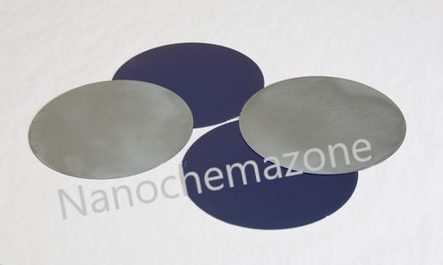
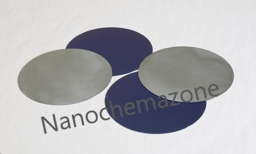
Silicon oxide wafer P-Type (2 inch)
₹0.00
Product Name: Silicon oxide wafer P-Type (2 inches)
| Product Name | Silicon oxide wafer P-Type (2 inches) |
| Cat. No. | NCZ-NSC318/20
|
| Diameter | 50.8+- 0.2 mm (2 inch)
|
| Oxide Thickness | 300 +- 20 nm (dry)
|
| Resistivity | (1-10 Ohm/sq).
|
| Thickness | 300+ 15 µm
|
| Orientation | <100>+- 0.5
|
Silicon oxide wafer P-Type (2 inches) Description
Provided in Single wafer case
Single Crystal Silicon for solar energy applications includes p-type and n-type silicon. Silicon Silicon-based photovoltaic cells (PV Cells) for solar energy are fabricated from a positively charged or p-type silicon layer underneath a negatively charged or n-type silicon layer. These layers can be produced from single crystal silicon material sold under the AE Solar Energy group. Most silicon-based PV solar cells are produced from polycrystalline silicon with single-crystal systems the next most common. Silicon Metal is also available as a polycrystalline powder for casting, amorphous silicon for deposition, disc, granules, ingot, pellets, pieces, powder, rod, sputtering target, wire, and other forms and custom shapes. Ultra-high purity and high purity forms also include submicron powder and nanoscale powder. Single Crystal Silicon is generally immediately available in most volumes.
Silicon oxide wafer P-Type (2 inches) RELATED INFORMATION
Storage Conditions:
Airtight sealed, avoid light, and keep dry at room temperature.
Please email us for the customization.
Email: contact@nanochemazone.com
Note: We supply different size ranges of nano and micron size powder as per the client’s requirements and also accept customization in various parameters.
Note: For pricing & ordering information, please contact us at sales@nanochemazone.com
Please contact us for quotes on Larger Quantities & Customization. E-mail: contact@nanochemazone.com
Customization:
If you are planning to order large quantities for your industrial and academic needs, please note that customization of parameters (such as size, length, purity, functionalities, etc.) are available upon request.
You must be logged in to post a review.
Related products
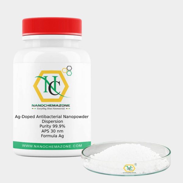
Ag-Doped Antibacterial Nanopowder Dispersion
Ag-Doped Antibacterial Nanopowder Dispersion
| Product | Ag-Doped Antibacterial Nanopowder Dispersion |
| CAS No. | 7440-22-4 |
| Appearance | Gary |
| Purity | 99.9% |
| APS | 30 nm(Can be customized) |
| Ingredient | Ag |
| Product Code | NCZ-NSC430/20 |
Ag-Doped Antibacterial Nanopowder Dispersion Description :
Ag-Doped Antibacterial Nanopowder Dispersion is nanoparticles of silver of between 1 nm and 100 nm in size. While frequently described as being 'silver' some are composed of a large percentage of silver oxide due to their large ratio of surface to bulk silver atoms.
Numerous shapes of Ag-doped Antibacterial Nanopowder Dispersion can be constructed depending on the application at hand. Commonly used silver nanoparticles are spherical, but diamond, octagonal, and thin sheets are also common.
Their extremely large surface area permits the coordination of a vast number of ligands. The properties of silver nanoparticles applicable to human treatments are under investigation in laboratory and animal studies, assessing potential efficacy, toxicity, and costs.
The most common methods for nanoparticle synthesis fall under the category of wet chemistry or the nucleation of particles within a solution.
This nucleation occurs when a silver ion complex, usually Ag-Doped Antibacterial Nanopowder Dispersion, is reduced to colloidal silver in the presence of a reducing agent. When the concentration increases enough, dissolved metallic silver ions bind together to form a stable surface.
The surface is energetically unfavorable when the cluster is small because the energy gained by decreasing the concentration of dissolved particles is not as high as the energy lost from creating a new surface.
When the cluster reaches a certain size, known as the critical radius, it becomes energetically favorable, and thus stable enough to continue to grow.
This nucleus then remains in the system and grows as more silver atoms diffuse through the solution and attach it to the surface.
When the dissolved concentration of atomic silver decreases enough, it is no longer possible for enough atoms to bind together to form a stable nucleus.
At this nucleation threshold, new nanoparticles stop being formed, and the remaining dissolved silver is absorbed by diffusion into the growing nanoparticles in the solution.
As the particles grow, other molecules in the solution diffuse and attach to the surface. This process stabilizes the surface energy of the particle and blocks new silver ions from reaching the surface.
The attachment of these capping/stabilizing agents slows and eventually stops the growth of the particle.
The most common capping ligands are trisodium citrate and polyvinylpyrrolidone (PVP), but many others are also used in varying conditions to synthesize particles with particular sizes, shapes, and surface properties.
There are many different wet synthesis methods, including the use of reducing sugars, nitrate reduction, reduction via sodium borohydride.
The silver mirror reaction, the polyol process, seed-mediated growth, and light-mediated growth. Each of these methods, or a combination of methods, will offer differing degrees of control over the size distribution as well as distributions of geometric arrangements of the nanoparticle.
Ag-Doped Antibacterial Nanopowder Dispersion Related Information
Storage Conditions: Airtight sealed, avoid light and keep dry at room temperature. Please contact us for customization and price inquiry Email: contact@nanochemazone.com Note: We supply different size ranges of Nano and micron as per the client’s requirements and also accept customization in various parameters.
Bismuth Metal Polycrystalline Powder
Product Name: Bismuth Metal Polycrystalline Powder
| Product | polycrystalline |
| CAS No. | 7440-69-9 |
| Appearance | brown Powder |
| Purity | 99.9% |
| APS | 1 – 5 Microns (Can be customized) |
| Ingredient | Bi |
| Product Code | NCZ-NSC-275/20 |
Calcium Magnesium Silicate
Calcium Magnesium Silicate
| Product |
Calcium Magnesium Silicate |
| CAS No. | N/A |
| Appearance | White |
| Purity | 99% |
| APS | 1-5µM (Can be customized) |
| Ingredient | CaMgSi2O6:Eu(2+) |
| Product Code | NCZ-NSC614/20 |
| Molecular Weight | 156.47 g/mol |
| Density | 2.9 g/cm3 |
| Melting Point | 2,130 °C (3,870 °F; 2,400 K) |
Calcium Magnesium Silicate Description
Calcium Chromate is generally immediately available in most volumes. Hydrate or anhydrous forms may be purchased. High purity, submicron and nanopowder forms may be considered. Nanochemazone produces to many standard grades when applicable, including Mil Spec (military grade); ACS, Reagent and Technical Grade; Food, Agricultural and Pharmaceutical Grade; Optical Grade, USP and EP/BP (European Pharmacopoeia/British Pharmacopoeia) and follows applicable ASTM testing standards. Typical and custom packaging is available. Additional technical, research and safety (MSDS) information is available as is a Reference Calculator for converting relevant units of measurement.
Related Information
Storage Conditions:
Airtight sealed, avoid light and keep dry at room temperature.
Please contact us for customization and price inquiry
Email: contact@nanochemazone.com
Note: We supply different size ranges of Nano and micron as per the client’s requirements and also accept customization in various parameters.
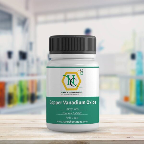
Copper Vanadium Oxide
Copper Vanadium Oxide
| Product |
Copper Vanadium Oxide |
| Colour | N/A |
| Purity | 99% |
| Particle Size | 1-5µM (customizable) |
| Ingredient/MF | CuO6V2 |
| Product Code | NCZ-CP-397/20 |
| CAS Number | 14958-34-0 |
| Density | N/A |
| Melting point | N/A |
| Boiling Point | N/A |
| Molecular Weight | 261.43 |
| Exact Mass | 260.787004 |
Related Information
Storage Conditions: Airtight sealed, avoid light and keep dry at room temperature. Please contact us for customization and price inquiry Email: contact@nanochemazone.com Note: We supply different size ranges of Nano and micron as per the client’s requirements and also accept customization in various parameters
D3O 10 mm Solid Sheet 10″x14.5″ (AERO) Unskived
D3O Sheets
D3O Sheets Also available in 2mm, 4mm, and 6mm Thickness.D3O Sheets with shock-absorbing properties
D3O® uses patented, patent-pending, and proprietary technologies to make rate-sensitive, soft, flexible materials with shock-absorbing properties.D3O Sheets D3O® foam sheets can be cut to size and applied to the body as an under-wrap to provide added protection to select body parts or to contusions without leaving the field for more than a few seconds. D3O® foam is soft and flexible and can be cut to any shape to match your specific needs.
Add D3O®’s patented impact protection to existing equipment by cutting your own padding. D3O® foams are made from cutting-edge smart molecules that remain soft and flexible until a force is applied causing the material to react on the molecular level by seizing up and binding together providing uncompromising impact protection.
D3O® set solid and mesh sheets reduce up to three times as much force as similar foam padding without the added bulk. Only 4mm of solid D3O® AERO out preforms 20mm of EVA foam in transmitted force testing by up to 60%. More than doubling the protective layer 10mm unskived AERO sheets are the ultimate side-line wrap.
To learn more about D3O® foam sheets and to get a glimpse at the raw testing data click the link below.
D3O-solid-mesh-sheet Pure Platinum Metal Sheet/Foil
Gallium Nitride Powder
Product Name: Gallium Nitride Powder
| Product | Gallium Nitride |
| CAS No. | 25617-97-4 |
| Appearance | Yellow Powder |
| Purity | 99.9% |
| APS | 1 – 5 Microns (Can be customized) |
| Ingredient | GaN |
| Product Code | NCZ-NSC-135/20 |

Lead Telluride Powder
Product Name: Lead Telluride Powder
| Product | Lead Telluride Powder |
| CAS No. | 1314-91-6 |
| Appearance | Grey Powder |
| Purity | 99.9% |
| APS | 1 – 5 Microns (Can be customized) |
| Ingredient | PbTe |
| Product Code | NCZ-NSC-140/20 |
Lead Telluride Description :
Lead tin telluride is a ternary alloy of lead, tin, and tellurium, generally made by alloying either tin into lead telluride or lead into tin telluride. It is a narrow bandgap semiconductor material.
The bandgap is tuned by varying the composition(x) in the material. SnTe can be alloyed with Pb (or PbTe with Sn) to tune the bandgap from (SnTe). Lead Telluride Powder important to note that unlike chalcogenides, e.g. cadmium, mercury, and zinc chalcogenides, the bandgap in Te does not change linearly between the two extremes. In contrast, as the composition (x) is increased, the bandgap decreases approach zero in the concentration regime (0.32–0.65 corresponding to temperature 4-300 K, respectively) and further increases towards the bulk bandgap of SnTe. Therefore, the lead-tin telluride alloys have narrower band gaps than their endpoint counterparts making lead tin telluride an ideal candidate for mid-infrared, 3–14 μm optoelectronic application.
Lead Telluride Powder has a positive temperature coefficient i.e. for a given composition x, the bandgap increases with temperature. Therefore, temperature stability has to be maintained while working with lead-tin telluride based laser. However, the advantage is that the operating wavelength of the laser can simply be tuned by varying the operating temperature.
The optical absorption coefficient of lead-tin telluride is typical ~750 cm−1 as compared to ~50 cm−1 for the extrinsic semiconductors such as doped silicon. The higher optical coefficient value not only ensures higher sensitivity but also reduces the spacing required between individual detector elements to prevent optical cross-talk making integrated circuit technology easily.
Lead Telluride Related Information
Storage Conditions: Airtight sealed, avoid light and keep dry at room temperature. Please email us for the customization. Email: contact@nanochemazone.com Note: We supply different size ranges of nano and micron size powder as per the client’s requirements and also accept customization in various parameters.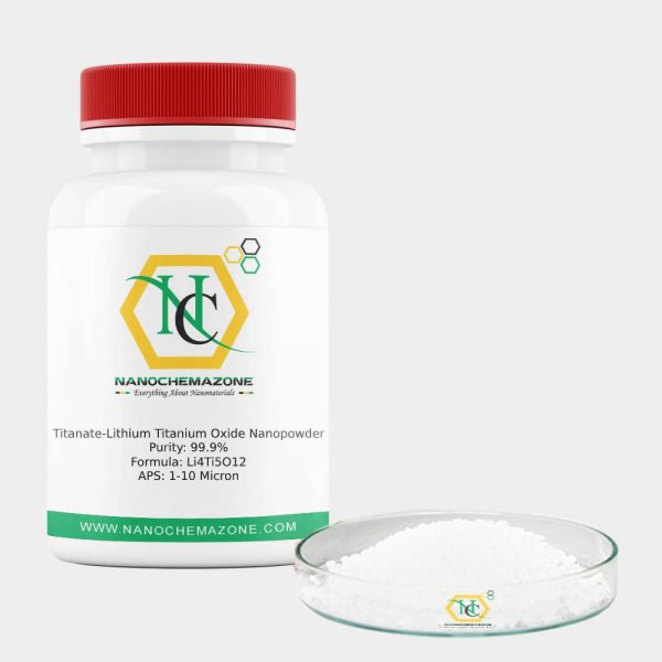
Titanate-Lithium Titanium Oxide Nanopowder
Titanate-Lithium Titanium Oxide Nanopowder
| Product | Titanate-Lithium Titanium Oxide Nanopowder |
| Colour | White |
| Purity | ≥ 99.99% |
| Particle size | 1-10 µM(customizable) |
| Ingredient/MF | Li4Ti5O12 |
| Product Code | NCZ-CK-189/20 |
| CAS Number | 12031-82-2/ 12031-95-7 |
Reviews
There are no reviews yet.