
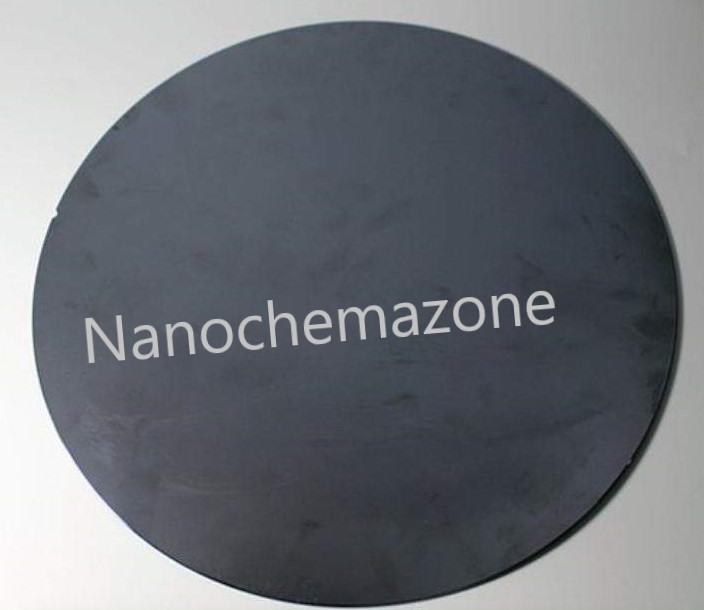
Single Crystal Silicon-Silicon dioxide Wafer
₹0.00
Single Crystal silicon-silicon dioxide Wafer
Product Name: Single Crystal silicon-silicon dioxide Wafer
| Product Name | Single Crystal silicon-silicon dioxide Wafer P-type (4 inches) |
| Cat No. | NCZ-NSC318/20 |
| Día | 100 mm (4 inches) |
| Orientation | <100> |
| Wafer thickness | 500 micrometer |
| Resistivity | <0.01 |
| Polished | Front Side Polished |
| Thickness | 300 nm (dry) |
| Purity | 99.9% |
| Formula | Si/SiO2 |
Single Crystal silicon-silicon dioxide Wafer P-type Description :
Provided in a single wafer case
Silicon oxide wafer SIO2 thin-film among semiconductor technology, SiO2 thin film layers are mainly used as dielectric material and more recently, they are integrated with MEMS (Micro Electro Mechanical Systems) devices. The simplest way to produce silicon oxide layers on silicon wafers is to oxidize silicon with oxygen.
Single Crystal silicon-silicon dioxide Wafer RELATED INFORMATION
Storage Conditions:
Airtight sealed, avoid light and keep dry at room temperature.
Please email us for the customization.
Email: contact@nanochemazone.com
Note: We supply different size ranges of nano and micron size powder as per the client’s requirements and also accept customization in various parameters.
Note: For pricing & ordering information, please contact us at sales@nanochemazone.com
Please contact us for quotes on Larger Quantities & Customization. E-mail: contact@nanochemazone.com
Customization:
If you are planning to order large quantities for your industrial and academic needs, please note that customization of parameters (such as size, length, purity, functionalities, etc.) are available upon request.
You must be logged in to post a review.
Related products

Antimony Tin oxide Powder
Antimony Tin oxide Powder
Product Name: Antimony Tin oxide powder| Product | Antimony Tin oxide powder |
| Colour | White |
| Purity | ≥ 99.9% |
| Particle size | 1-10 µM (customizable) |
| Ingredient/MF | SnO2, Sb2O3 |
| Product Code | NCZ-CM-176/20 |
| CAS Number | 18282-10-5/1309-64-4 |
- ATO has excellent electrical and optical properties that are widely used as good electrical conductivity, also as an antistatic agent widely used in paint, chemical fiber, polymer film field.
- ATO has good insulation properties. Used the ATO coating to be made of automotive glass is an excellent effect of shielding and reflecting infrared radiation.
- ATO with super fine conductive properties can be used in paints, textiles, plastics, and other fields, the direct mixing of liquid and configuration system, good compatibility.
- ATO has excellent electrical and optical properties. Used as an antistatic agent is widely used in paint, chemical fiber, polymer film field.
Calcium Magnesium Silicate
Calcium Magnesium Silicate
| Product |
Calcium Magnesium Silicate |
| CAS No. | N/A |
| Appearance | White |
| Purity | 99% |
| APS | 1-5µM (Can be customized) |
| Ingredient | CaMgSi2O6:Eu(2+) |
| Product Code | NCZ-NSC614/20 |
| Molecular Weight | 156.47 g/mol |
| Density | 2.9 g/cm3 |
| Melting Point | 2,130 °C (3,870 °F; 2,400 K) |
Calcium Magnesium Silicate Description
Calcium Chromate is generally immediately available in most volumes. Hydrate or anhydrous forms may be purchased. High purity, submicron and nanopowder forms may be considered. Nanochemazone produces to many standard grades when applicable, including Mil Spec (military grade); ACS, Reagent and Technical Grade; Food, Agricultural and Pharmaceutical Grade; Optical Grade, USP and EP/BP (European Pharmacopoeia/British Pharmacopoeia) and follows applicable ASTM testing standards. Typical and custom packaging is available. Additional technical, research and safety (MSDS) information is available as is a Reference Calculator for converting relevant units of measurement.
Related Information
Storage Conditions:
Airtight sealed, avoid light and keep dry at room temperature.
Please contact us for customization and price inquiry
Email: contact@nanochemazone.com
Note: We supply different size ranges of Nano and micron as per the client’s requirements and also accept customization in various parameters.

Gallium Nitride Powder
Product Name: Gallium Nitride Powder
| Product | Gallium Nitride |
| CAS No. | 25617-97-4 |
| Appearance | Yellow Powder |
| Purity | 99.9% |
| APS | 1 – 5 Microns (Can be customized) |
| Ingredient | GaN |
| Product Code | NCZ-NSC-135/20 |

Silicon oxide wafer P-Type (2 inch)
Product Name: Silicon oxide wafer P-Type (2 inches)
| Product Name | Silicon oxide wafer P-Type (2 inches) |
| Cat. No. | NCZ-NSC318/20 |
| Diameter | 50.8+- 0.2 mm (2 inch) |
| Oxide Thickness | 300 +- 20 nm (dry) |
| Resistivity | (1-10 Ohm/sq). |
| Thickness | 300+ 15 µm |
| Orientation | <100>+- 0.5 |
Silicon oxide wafer P-Type (2 inches) Description
Provided in Single wafer caseSingle Crystal Silicon for solar energy applications includes p-type and n-type silicon. Silicon Silicon-based photovoltaic cells (PV Cells) for solar energy are fabricated from a positively charged or p-type silicon layer underneath a negatively charged or n-type silicon layer. These layers can be produced from single crystal silicon material sold under the AE Solar Energy group. Most silicon-based PV solar cells are produced from polycrystalline silicon with single-crystal systems the next most common. Silicon Metal is also available as a polycrystalline powder for casting, amorphous silicon for deposition, disc, granules, ingot, pellets, pieces, powder, rod, sputtering target, wire, and other forms and custom shapes. Ultra-high purity and high purity forms also include submicron powder and nanoscale powder. Single Crystal Silicon is generally immediately available in most volumes.
Silicon oxide wafer P-Type (2 inches) RELATED INFORMATION
Storage Conditions: Airtight sealed, avoid light, and keep dry at room temperature. Please email us for the customization. Email: contact@nanochemazone.com Note: We supply different size ranges of nano and micron size powder as per the client’s requirements and also accept customization in various parameters.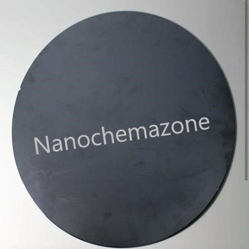
Single Crystal Silicon Wafer Diameter Intrinsic (4-inch)
Single Crystal Silicon Wafer Diameter Intrinsic (4-inch)
Product Name: Single Crystal Silicon Wafer Diameter Intrinsic (4-inch)
| Product Name | Single Crystal Silicon Wafer |
| Cat No. | NCZ-NSC327/20 |
| Diameter | 4 inches |
| Doping | undoped |
| Thickness | 400~415+/-10um |
| Resistivity | 4000 5000 ohms.cm Undoped |
| Orientation | <100>+/-0.5 |
| Polishing | one side polished |
| Application | Research Material |
| Thickness | 525 Micron |
| Resistivity | 1-10 ohm-cm |
| Polished | Single side polished |
Single Crystal Silicon Wafer thickness Is determined by the mechanical strength of the material used the wafer must be thick enough to support its own weight without cracking during handling. Wafers are grown from crystal having a regular crystal structure, with silicon having a diamond cubic structure. Orientation is defined by the Miller index with (100) or (111) faces being the most common for silicon. Ion implantation depends on the wafer’s crystal orientation since each direction offers distinct paths the transport.
Note: SSP = Single Side Polished, DSP = Double Side Polished, E = Etched, C = AsCut, Material - CZ unless noted, L = Lapped, Und = Undoped (Intrinsic)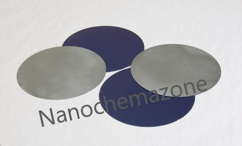
Single Crystal Silicon Wafer Intrinsic (2 Inch)
Single Crystal Silicon Wafer Intrinsic (2 Inch)
Product Name: Single Crystal Silicon Wafer Intrinsic (2 Inch)
| Product Name | Single Crystal Silicon Wafer Intrinsic (2 Inch) |
| Cat No. | NCZ-NSC328/20 |
| Size | 50.8+/- 0.2mm, |
| Thickness | 430+/-10um |
| Undoped | Intrinsic |
| Resistivity | 2000~4000Ω.cm |
| Orientation | <100>+/-0.5° |
| Polishing | One Side Polished |
Single Crystal Silicon Wafer Intrinsic is the most widely used semiconductor material as a substrate material due to its excellent machinability, mechanical stability, and the potential to combine sensing elements and electronics on the same substrate.
Circular wafers made of silicon are used as a substrate in most MEMS sensors. The crystal orientation should be known before manufacturing since silicon has orientation-dependent properties such as piezoresistivity coefficients and etching rates. The common orientation is (100) where the numbers represent Miller indices.
As an example, (100) wafer that has a primary flat side as an indication of < 110 > direction. When a piezoresistive element is placed on a (100) wafer, the orientation should be parallel to < 110 > direction if the piezoresistivity coefficients in that direction are intended to be utilized.
Single crystal silicon wafer Intrinsic (2-inch)
Single crystal silicon wafer Intrinsic (2-inch)
Product Name: Single crystal silicon wafer Intrinsic (2-inch)
| Product Name | Single crystal silicon wafer Intrinsic (2-inch) |
| Cat No. | NCZ-NSC329/20 |
| Diameter | 2 inch |
| Doping | Intrinsic |
| Resistivity | (>1000ohm/sq.) |
| Thickness | 400µm |
| Orientation | 100 |
| Polished | Single side polished |
Single crystal silicon wafer Intrinsic (2-inch) is the most widely used semiconductor material as a substrate material due to its excellent machinability, mechanical stability, and the potential to combine sensing elements and electronics on the same substrate. Circular wafers made of silicon are used as a substrate in most MEMS sensors.
The crystal orientation should be known before manufacturing since silicon has orientation-dependent properties such as piezoresistivity coefficients and etching rates. The common orientation is (100) where the numbers represent Miller indices.
As an example, (100) wafer that has a primary flat side as an indication of < 110 > direction. When a piezoresistive element is placed on a (100) wafer, the orientation should be parallel to < 110 > direction if the piezoresistivity coefficients in that direction are intended to be utilized.
Please email us for the customization. Email: contact@nanochemazone.com Please contact us for customization and price inquiry Note: We supply different size ranges of Nano and micron as per the client’s requirements and also accept customization in the various parameters.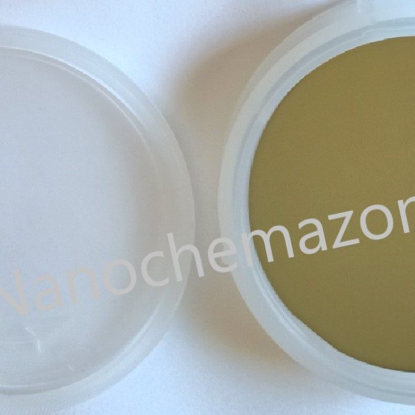
Single Crystal Silicon Wafer P-type,
Single Crystal Silicon Wafer P-type,
| Product Name | Single Crystal Silicon Wafer P-type |
| Cat No. | NCZ-NSC332/20 |
| Día | 3 inch |
| Diameter | 76.2mm ± 0.3mm (3 inches) |
| Type | P |
| Orientation | <100> |
| Thickness | 400±10um |
| Resistivity | 1-10 ohm-cm |
| Polished | Single side polished |
Reviews
There are no reviews yet.