 1")
Single Crystal Silicon Wafer N-Type
₹0.00
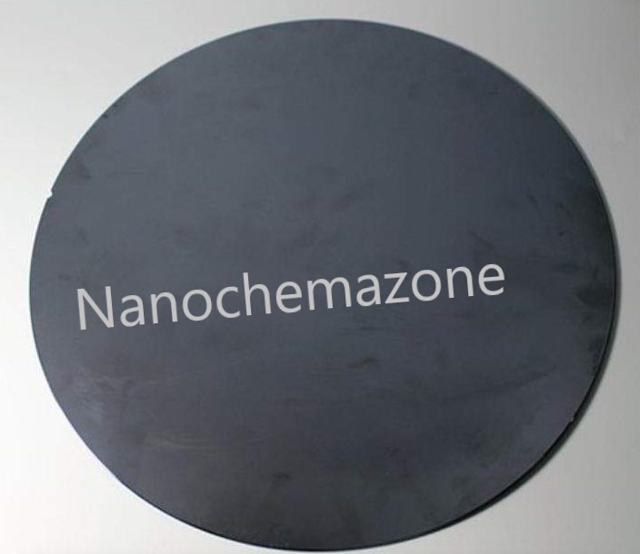
Single Crystal Silicon Wafer N-Type (1 inch)
Product Name: Single Crystal Silicon Wafer N-Type (1 inch)
| Product Name | Single Crystal Silicon Wafer N-Type (1 inch) |
| Cat No. | NCZ-NSC330/20 |
| Size | 1 inch |
| Thickness | 300-380 micro-meter |
| Type | N-type |
| Dopant | Phosphorus |
| Resistivity | 1-10 ohm/cm |
| Surface | Single side polished |
| Boling Point | 2355 °C (lit.) |
| Melting Point | 1240 °C,1410 °C (lit.) |
| Density | 2.33 g/mL at 25 °C (lit.) |
| Semiconductor Properties | <100>, N-type |
| SMILES string | [Si] |
Physical properties:
0 vortex defects. Etch pitch density (EPD) < 100 (cm-2). Resistivity 100 – 3000 Ωcm.
Oxygen content: ≤ 1~1.8 x 10¹⁸ /cm3; Carbon content: ≤ 5 x 10¹⁶ /cm3; Boule diameter: 1~8 ″
Description:
Single Crystal Silicon Wafer N-Type (1 inch). We have heated polished doped single-crystal silicon wafers in a single-mode microwave cavity to temperatures where surface to surface bonding occurred. The absorption of microwaves and heating of the wafers is attributed to the inclusion of n-type or p-type impurities into these substrates.
A cylindrical cavity TM (sub 010) standing wave mode was used to irradiate samples of various geometry at positions of high magnetic field. This process was conducted in a vacuum to exclude plasma effects.
This initial study suggests that the inclusion of impurities in single crystal silicon significantly improved its microwave absorption (loss factor) to a point where heating silicon wafers directly can be accomplished in minimal time. Bonding of these substrates, however, occurs only at points of intimate surface to surface contact. The inclusion of a thin metallic layer on the surfaces enhances the bonding process.
Please email us for the customization.
Email: contact@nanochemazone.com
Please contact us for customization and price inquiry
Note: We supply different size ranges of Nano and micron as per the client’s requirements and also accept customization in the various parameters
Note: For pricing & ordering information, please contact us at sales@nanochemazone.com
Please contact us for quotes on Larger Quantities & Customization. E-mail: contact@nanochemazone.com
Customization:
If you are planning to order large quantities for your industrial and academic needs, please note that customization of parameters (such as size, length, purity, functionalities, etc.) are available upon request.
You must be logged in to post a review.
Related products

Bismuth Metal Polycrystalline Powder
Product Name: Bismuth Metal Polycrystalline Powder
| Product | polycrystalline |
| CAS No. | 7440-69-9 |
| Appearance | brown Powder |
| Purity | 99.9% |
| APS | 1 – 5 Microns (Can be customized) |
| Ingredient | Bi |
| Product Code | NCZ-NSC-275/20 |
Description :
Bismuth compounds account for about half the production of bismuth. They are used in cosmetics, pigments, and a few pharmaceuticals, notably bismuth subsalicylate, used to treat diarrhea. Bismuth's unusual propensity to expand as it solidifies is responsible for some of its uses, such as in the casting of printing type. Bismuth has unusually low toxicity for heavy metal. As the toxicity of lead has become more apparent in recent years, there is increasing use of bismuth alloys presently about a third of bismuth production) as a replacement for lead.
RELATED INFORMATION
Storage Conditions:
Airtight sealed, avoid light, and keep dry at room temperature.
Please contact us for customization and price inquiry
Email: contact@nanochemazone.com
Note: We supply different size ranges of Nano and micron as per the client’s requirements and also accept customization in various parameters.

D3O 10 mm Solid Sheet 10″x14.5″ (AERO) Unskived
D3O Sheets
D3O Sheets Also available in 2mm, 4mm, and 6mm Thickness.
D3O Sheets with shock-absorbing properties
D3O® uses patented, patent-pending, and proprietary technologies to make rate-sensitive, soft, flexible materials with shock-absorbing properties.
D3O Sheets D3O® foam sheets can be cut to size and applied to the body as an under-wrap to provide added protection to select body parts or to contusions without leaving the field for more than a few seconds. D3O® foam is soft and flexible and can be cut to any shape to match your specific needs.
Add D3O®’s patented impact protection to existing equipment by cutting your own padding. D3O® foams are made from cutting-edge smart molecules that remain soft and flexible until a force is applied causing the material to react on the molecular level by seizing up and binding together providing uncompromising impact protection.
D3O® set solid and mesh sheets reduce up to three times as much force as similar foam padding without the added bulk. Only 4mm of solid D3O® AERO out preforms 20mm of EVA foam in transmitted force testing by up to 60%. More than doubling the protective layer 10mm unskived AERO sheets are the ultimate side-line wrap.
To learn more about D3O® foam sheets and to get a glimpse at the raw testing data click the link below.

Gallium Nitride Powder
Product Name: Gallium Nitride Powder
| Product | Gallium Nitride |
| CAS No. | 25617-97-4 |
| Appearance | Yellow Powder |
| Purity | 99.9% |
| APS | 1 – 5 Microns (Can be customized) |
| Ingredient | GaN |
| Product Code | NCZ-NSC-135/20 |
Description :
Materials research and application of the current global semiconductor research front and hot is the development of microelectronic devices, optoelectronic devices of new semiconductor materials. It has a wide direct bandgap, strong atomic bonds, high thermal conductivity, good chemical stability (almost no acid corrosion), and other properties and strong anti-radiation ability in optoelectronics, high temperature, and high power devices and high-Frequency microwave device applications have a broad prospect.
RELATED INFORMATION
Storage Conditions:
Airtight sealed, avoid light, and keep dry at room temperature.
Please email us for the customization.
Email: contact@nanochemazone.com
Note: We supply different size ranges of nano and micron size powder as per the client’s requirements and also accept customization in various parameters.
Iron Magnesium Zinc Oxide
Iron Magnesium Zinc Oxide
Product |
Iron Magnesium Zinc Oxide |
| Colour | N/A |
| Purity | 99% |
| Particle Size | 1-5µM (Customizable) |
| Ingredient/MF | MgxZn1-xFe2O4 |
| Product Code | NCZ-CP-367/20 |
| CAS Number | 15552-14-4 |
| Density | N/A |
| Melting point | N/A |
| Boiling Point | N/A |
| Molecular Weight | N/A |
| Exact Mass | N/A |
Iron Magnesium Zinc Oxide Description
Magnesium is a Block S, Group 2, Period 3 element with an atomic mass of 24.3050. The number of electrons in each of Magnesium's shells is [2, 8, 2] and its electron configuration is [Ne] 3s2. The magnesium atom has a radius of 160 pm and a Van der Waals radius of 173 pm.
Magnesium was discovered by Joseph Black in 1775 and first isolated by Sir Humphrey Davy in 1808. Magnesium is the eighth most abundant element in the earth's crust and the fourth most common element in the earth as a whole.
In its elemental form, magnesium has a shiny grey metallic appearance and is an extremely reactive. It is can be found in minerals such as brucite, carnallite, dolomite, magnesite, olivine and talc. Commercially, magnesium is primarily used in the creation of strong and lightweight aluminum-magnesium alloys, which have numerous advantages in industrial applications. The name "Magnesium" originates from a Greek district in Thessaly called Magnesia.
Iron:
Iron is a Block D, Group 8, Period 4 element with an atomic weight of 55.845. The number of electrons in each of Iron's shells is 2, 8, 14, 2 and its electron configuration is [Ar] 3d6 4s2. The iron atom has a radius of 126 pm and a Van der Waals radius of 194 pm. Iron was discovered by humans before 5000 BC. In its elemental form, iron has a lustrous grayish metallic appearance. Iron is the fourth most common element in the Earth's crust and the most common element by mass forming the earth as a whole.
Iron is rarely found as a free element, since it tends to oxidize easily; it is usually found in minerals such as magnetite, hematite, goethite, limonite, or siderite. Though pure iron is typically soft, the addition of carbon creates the alloy known as steel, which is significantly stronger.
Zinc:
Zinc is a Block D, Group 12, Period 4 element with an atomic weight of 65.38. The number of electrons in each of zinc's shells is 2, 8, 18, 2, and its electron configuration is [Ar] 3d10 4s2. The zinc atom has a radius of 134 pm and a Van der Waals radius of 210 pm. Zinc was discovered by Indian metallurgists prior to 1000 BC and first recognized as a unique element by Rasaratna Samuccaya in 800. Zinc was first isolated by Andreas Marggraf in 1746. In its elemental form, zinc has a silver-gray appearance.
It is brittle at ordinary temperatures but malleable at 100 °C to 150 °C. It is a fair conductor of electricity, and burns in air at high red producing white clouds of the oxide. Zinc is mined from sulfidic ore deposits. It is the 24th most abundant element in the earth's crust and the fourth most common metal in use (after iron, aluminum, and copper). The name zinc originates from the German word "zin," meaning tin.
Related Information
Please email us for the customization.
Email: contact@nanochemazone.com
Please contact us for customization and price inquiry
Note: We supply different size ranges of Nano and micron as per the client’s requirements and also accept customization in various parameters.
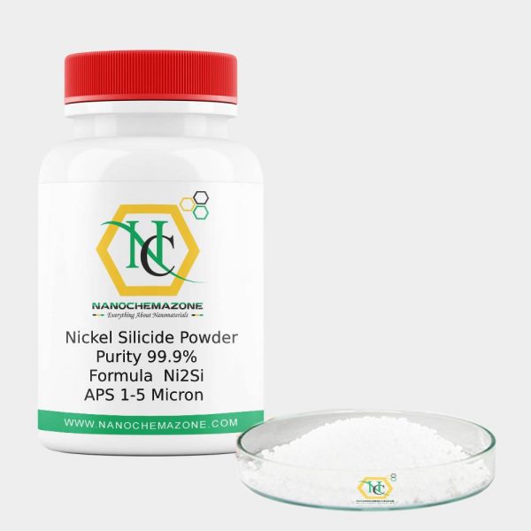
Nickel Silicide Powder
Nickel Silicide Powder
Product Name: Nickel Silicide Powder
| Product | Nickel Silicide Powder |
| CAS No | 12059-14-2 |
| Appearance | White Powder |
| Purity | 99.9% |
| APS | 1 – 5 Microns (Can be customized) |
| Ingredient | Ni2Si |
| Product Code | NCZ-NSC-133/20 |
Nickel Silicide Powder Related Information:
Nickel Silicide Powder: The reaction between SiC with chemically plated nickel on its surface has been investigated. X-ray analysis gave a good number of lattice parameters for Ni 3Si, a = 0.3522nm, and has good agreement with the index. The surface layer of Ni diffuses into the SiC and exothermically forms Ni 3Si in a defined temperature range, producing free carbon which could be deleterious to the properties.
A reaction is evident at temperatures 900°C and 1350°C with an increasing trend. The mechanism of sintering which is shown to be a reaction sintered transient-liquid phase method was determined by thermal analysis and metallographic techniques. The strength, hardness, and density properties of sintered Ni /Al (Liquid) + SiC composites are also reported.
Storage Conditions:
Airtight sealed, avoid light and keep dry at room temperature.
Please email us for the customization.
Email: contact@nanochemazone.com
Note: We supply different size ranges of nano and micron size powder as per the client’s requirements and also accept customization in various parameters.
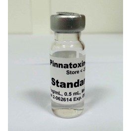
Pinnatoxin-G CAS: 1312711-74-2
Pinnatoxin-G
| Product Name | Pinnatoxin-G |
| Cat No | NCZ-000-101 |
| CAS No | 1312711-74-2 |
| Synonyms | Pinnatoxin G |
| Molecular Formula | C42H63NO7 |
| Molecular Weight | 693.95 |
Pinnatoxin-G CAS: 1312711-74-2
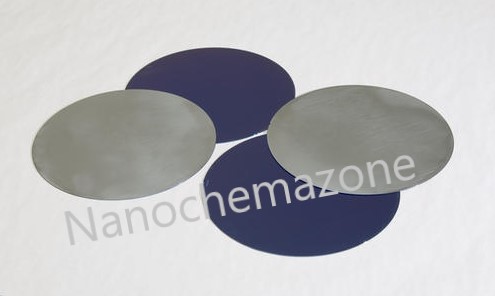
Single crystal silicon wafer Intrinsic (2-inch)
Single crystal silicon wafer Intrinsic (2-inch)
Product Name: Single crystal silicon wafer Intrinsic (2-inch)
| Product Name | Single crystal silicon wafer Intrinsic (2-inch) |
| Cat No. | NCZ-NSC329/20 |
| Diameter | 2 inch |
| Doping | Intrinsic |
| Resistivity | (>1000ohm/sq.) |
| Thickness | 400µm |
| Orientation | 100 |
| Polished | Single side polished |
Provided in a Single wafer case:
Description:
Single crystal silicon wafer Intrinsic (2-inch) is the most widely used semiconductor material as a substrate material due to its excellent machinability, mechanical stability, and the potential to combine sensing elements and electronics on the same substrate. Circular wafers made of silicon are used as a substrate in most MEMS sensors.
The crystal orientation should be known before manufacturing since silicon has orientation-dependent properties such as piezoresistivity coefficients and etching rates. The common orientation is (100) where the numbers represent Miller indices.
As an example, (100) wafer that has a primary flat side as an indication of < 110 > direction. When a piezoresistive element is placed on a (100) wafer, the orientation should be parallel to < 110 > direction if the piezoresistivity coefficients in that direction are intended to be utilized.
Please email us for the customization.
Email: contact@nanochemazone.com
Please contact us for customization and price inquiry
Note: We supply different size ranges of Nano and micron as per the client’s requirements and also accept customization in the various parameters.
Single crystal silicon wafer N-type (2 inch)
Single crystal silicon wafer N-type (2 inch)
Product Name: Single crystal silicon wafer N-type (2 inch)
| Product Name | Single crystal silicon wafer N-type (2 inch) |
| Cat No. | NCZ-NSC332/20 |
| Diameter | 2 inch |
| Doping | N type |
| Resistivity | (1-10 Ohm/sq). |
| Thickness | 290 + 10 µm |
| Orientation | 100 |
| Polished | Single side polished |
| Form | crystalline (cubic (a = 5.4037) |
| Polished | wafer (single side polished |
| does not contain | dopant |
| dia | 2 inch |
| Thickness | 0.5 mm |
| Boling Point | 2355 °C (lit.) |
| Melting Point | 1410 °C (lit.) |
| Density | 2.33 g/mL at 25 °C (lit.) |
| Semiconductor properties | <100>, N-type |
| SMILES string | [Si] |
Description:
Single crystal silicon wafer N-type (2 inch) NanoChemazone Supplies provides both standard and customized high-quality single crystals, wafers and substrates for a wide range of applications such as LED, ferroelectric, piezoelectric, electro-optical, photonics, high power electronics, and high-frequency power devices, just to name a few. Customized crystal growth, precision machining, and coating services are available. Please contact us today to discuss your project requirements.
Please email us for the customization.
Email: contact@nanochemazone.com
Please contact us for customization and price inquiry
Note: We supply different size ranges of Nano and micron as per the client’s requirements and also accept customization in the various parameters.
Reviews
There are no reviews yet.