

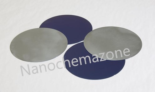
Single Crystal Silicon Wafer N-Type
₹0.00
Single Crystal Silicon Wafer N-Type (1 inch)
Product Name: Single Crystal Silicon Wafer N-Type (1 inch)
| Product Name | Single Crystal Silicon Wafer N-Type (1 inch) |
| Cat No. | NCZ-NSC330/20 |
| Size | 1 inch |
| Thickness | 300-380 micro-meter |
| Type | N-type |
| Dopant | Phosphorus |
| Resistivity | 1-10 ohm/cm |
| Surface | Single side polished |
| Boling Point | 2355 °C (lit.) |
| Melting Point | 1240 °C,1410 °C (lit.) |
| Density | 2.33 g/mL at 25 °C (lit.) |
| Semiconductor Properties | <100>, N-type |
| SMILES string | [Si] |
Physical properties:
0 vortex defects. Etch pitch density (EPD) < 100 (cm-2). Resistivity 100 – 3000 Ωcm.
Oxygen content: ≤ 1~1.8 x 10¹⁸ /cm3; Carbon content: ≤ 5 x 10¹⁶ /cm3; Boule diameter: 1~8 ″
Description:
Single Crystal Silicon Wafer N-Type (1 inch). We have heated polished doped single-crystal silicon wafers in a single-mode microwave cavity to temperatures where surface to surface bonding occurred. The absorption of microwaves and heating of the wafers is attributed to the inclusion of n-type or p-type impurities into these substrates.
A cylindrical cavity TM (sub 010) standing wave mode was used to irradiate samples of various geometry at positions of high magnetic field. This process was conducted in a vacuum to exclude plasma effects.
This initial study suggests that the inclusion of impurities in single crystal silicon significantly improved its microwave absorption (loss factor) to a point where heating silicon wafers directly can be accomplished in minimal time. Bonding of these substrates, however, occurs only at points of intimate surface to surface contact. The inclusion of a thin metallic layer on the surfaces enhances the bonding process.
Please email us for the customization.
Email: contact@nanochemazone.com
Please contact us for customization and price inquiry
Note: We supply different size ranges of Nano and micron as per the client’s requirements and also accept customization in the various parameters
Note: For pricing & ordering information, please contact us at sales@nanochemazone.com
Please contact us for quotes on Larger Quantities & Customization. E-mail: contact@nanochemazone.com
Customization:
If you are planning to order large quantities for your industrial and academic needs, please note that customization of parameters (such as size, length, purity, functionalities, etc.) are available upon request.
You must be logged in to post a review.
Related products
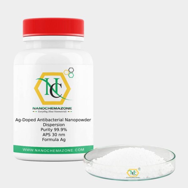
Ag-Doped Antibacterial Nanopowder Dispersion
Ag-Doped Antibacterial Nanopowder Dispersion
| Product | Ag-Doped Antibacterial Nanopowder Dispersion |
| CAS No. | 7440-22-4 |
| Appearance | Gary |
| Purity | 99.9% |
| APS | 30 nm(Can be customized) |
| Ingredient | Ag |
| Product Code | NCZ-NSC430/20 |
Ag-Doped Antibacterial Nanopowder Dispersion Description :
Ag-Doped Antibacterial Nanopowder Dispersion is nanoparticles of silver of between 1 nm and 100 nm in size. While frequently described as being 'silver' some are composed of a large percentage of silver oxide due to their large ratio of surface to bulk silver atoms.
Numerous shapes of Ag-doped Antibacterial Nanopowder Dispersion can be constructed depending on the application at hand. Commonly used silver nanoparticles are spherical, but diamond, octagonal, and thin sheets are also common.
Their extremely large surface area permits the coordination of a vast number of ligands. The properties of silver nanoparticles applicable to human treatments are under investigation in laboratory and animal studies, assessing potential efficacy, toxicity, and costs.
The most common methods for nanoparticle synthesis fall under the category of wet chemistry or the nucleation of particles within a solution.
This nucleation occurs when a silver ion complex, usually Ag-Doped Antibacterial Nanopowder Dispersion, is reduced to colloidal silver in the presence of a reducing agent. When the concentration increases enough, dissolved metallic silver ions bind together to form a stable surface.
The surface is energetically unfavorable when the cluster is small because the energy gained by decreasing the concentration of dissolved particles is not as high as the energy lost from creating a new surface.
When the cluster reaches a certain size, known as the critical radius, it becomes energetically favorable, and thus stable enough to continue to grow.
This nucleus then remains in the system and grows as more silver atoms diffuse through the solution and attach it to the surface.
When the dissolved concentration of atomic silver decreases enough, it is no longer possible for enough atoms to bind together to form a stable nucleus.
At this nucleation threshold, new nanoparticles stop being formed, and the remaining dissolved silver is absorbed by diffusion into the growing nanoparticles in the solution.
As the particles grow, other molecules in the solution diffuse and attach to the surface. This process stabilizes the surface energy of the particle and blocks new silver ions from reaching the surface.
The attachment of these capping/stabilizing agents slows and eventually stops the growth of the particle.
The most common capping ligands are trisodium citrate and polyvinylpyrrolidone (PVP), but many others are also used in varying conditions to synthesize particles with particular sizes, shapes, and surface properties.
There are many different wet synthesis methods, including the use of reducing sugars, nitrate reduction, reduction via sodium borohydride.
The silver mirror reaction, the polyol process, seed-mediated growth, and light-mediated growth. Each of these methods, or a combination of methods, will offer differing degrees of control over the size distribution as well as distributions of geometric arrangements of the nanoparticle.
Ag-Doped Antibacterial Nanopowder Dispersion Related Information
Storage Conditions: Airtight sealed, avoid light and keep dry at room temperature. Please contact us for customization and price inquiry Email: contact@nanochemazone.com Note: We supply different size ranges of Nano and micron as per the client’s requirements and also accept customization in various parameters.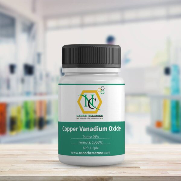
Copper Vanadium Oxide
Copper Vanadium Oxide
| Product |
Copper Vanadium Oxide |
| Colour | N/A |
| Purity | 99% |
| Particle Size | 1-5µM (customizable) |
| Ingredient/MF | CuO6V2 |
| Product Code | NCZ-CP-397/20 |
| CAS Number | 14958-34-0 |
| Density | N/A |
| Melting point | N/A |
| Boiling Point | N/A |
| Molecular Weight | 261.43 |
| Exact Mass | 260.787004 |
Related Information
Storage Conditions: Airtight sealed, avoid light and keep dry at room temperature. Please contact us for customization and price inquiry Email: contact@nanochemazone.com Note: We supply different size ranges of Nano and micron as per the client’s requirements and also accept customization in various parameters
D3O 10 mm Solid Sheet 10″x14.5″ (AERO) Unskived
D3O Sheets
D3O Sheets Also available in 2mm, 4mm, and 6mm Thickness.D3O Sheets with shock-absorbing properties
D3O® uses patented, patent-pending, and proprietary technologies to make rate-sensitive, soft, flexible materials with shock-absorbing properties.D3O Sheets D3O® foam sheets can be cut to size and applied to the body as an under-wrap to provide added protection to select body parts or to contusions without leaving the field for more than a few seconds. D3O® foam is soft and flexible and can be cut to any shape to match your specific needs.
Add D3O®’s patented impact protection to existing equipment by cutting your own padding. D3O® foams are made from cutting-edge smart molecules that remain soft and flexible until a force is applied causing the material to react on the molecular level by seizing up and binding together providing uncompromising impact protection.
D3O® set solid and mesh sheets reduce up to three times as much force as similar foam padding without the added bulk. Only 4mm of solid D3O® AERO out preforms 20mm of EVA foam in transmitted force testing by up to 60%. More than doubling the protective layer 10mm unskived AERO sheets are the ultimate side-line wrap.
To learn more about D3O® foam sheets and to get a glimpse at the raw testing data click the link below.
D3O-solid-mesh-sheet Pure Platinum Metal Sheet/Foil
Iron Magnesium Zinc Oxide
Iron Magnesium Zinc Oxide
Product |
Iron Magnesium Zinc Oxide |
| Colour | N/A |
| Purity | 99% |
| Particle Size | 1-5µM (Customizable) |
| Ingredient/MF | MgxZn1-xFe2O4 |
| Product Code | NCZ-CP-367/20 |
| CAS Number | 15552-14-4 |
| Density | N/A |
| Melting point | N/A |
| Boiling Point | N/A |
| Molecular Weight | N/A |
| Exact Mass | N/A |
Iron Magnesium Zinc Oxide Description
Magnesium is a Block S, Group 2, Period 3 element with an atomic mass of 24.3050. The number of electrons in each of Magnesium's shells is [2, 8, 2] and its electron configuration is [Ne] 3s2. The magnesium atom has a radius of 160 pm and a Van der Waals radius of 173 pm.
Magnesium was discovered by Joseph Black in 1775 and first isolated by Sir Humphrey Davy in 1808. Magnesium is the eighth most abundant element in the earth's crust and the fourth most common element in the earth as a whole.
In its elemental form, magnesium has a shiny grey metallic appearance and is an extremely reactive. It is can be found in minerals such as brucite, carnallite, dolomite, magnesite, olivine and talc. Commercially, magnesium is primarily used in the creation of strong and lightweight aluminum-magnesium alloys, which have numerous advantages in industrial applications. The name "Magnesium" originates from a Greek district in Thessaly called Magnesia.
Iron:
Iron is a Block D, Group 8, Period 4 element with an atomic weight of 55.845. The number of electrons in each of Iron's shells is 2, 8, 14, 2 and its electron configuration is [Ar] 3d6 4s2. The iron atom has a radius of 126 pm and a Van der Waals radius of 194 pm. Iron was discovered by humans before 5000 BC. In its elemental form, iron has a lustrous grayish metallic appearance. Iron is the fourth most common element in the Earth's crust and the most common element by mass forming the earth as a whole.
Iron is rarely found as a free element, since it tends to oxidize easily; it is usually found in minerals such as magnetite, hematite, goethite, limonite, or siderite. Though pure iron is typically soft, the addition of carbon creates the alloy known as steel, which is significantly stronger.
Zinc:
Zinc is a Block D, Group 12, Period 4 element with an atomic weight of 65.38. The number of electrons in each of zinc's shells is 2, 8, 18, 2, and its electron configuration is [Ar] 3d10 4s2. The zinc atom has a radius of 134 pm and a Van der Waals radius of 210 pm. Zinc was discovered by Indian metallurgists prior to 1000 BC and first recognized as a unique element by Rasaratna Samuccaya in 800. Zinc was first isolated by Andreas Marggraf in 1746. In its elemental form, zinc has a silver-gray appearance.
It is brittle at ordinary temperatures but malleable at 100 °C to 150 °C. It is a fair conductor of electricity, and burns in air at high red producing white clouds of the oxide. Zinc is mined from sulfidic ore deposits. It is the 24th most abundant element in the earth's crust and the fourth most common metal in use (after iron, aluminum, and copper). The name zinc originates from the German word "zin," meaning tin.
Related Information
Please email us for the customization.
Email: contact@nanochemazone.com
Please contact us for customization and price inquiry
Note: We supply different size ranges of Nano and micron as per the client’s requirements and also accept customization in various parameters.
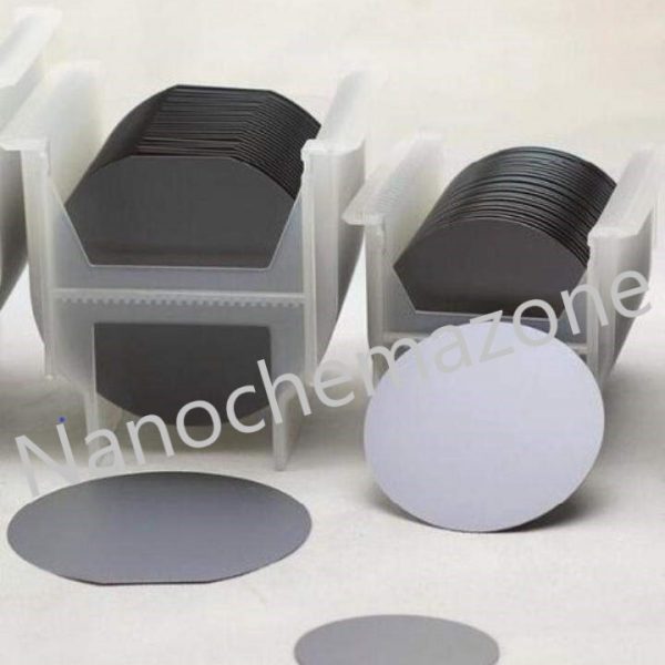
Single crystal silicon wafer N-type (2 inch)
Single crystal silicon wafer N-type (2 inch)
Product Name: Single crystal silicon wafer N-type (2 inch)
| Product Name | Single crystal silicon wafer N-type (2 inch) |
| Cat No. | NCZ-NSC332/20 |
| Diameter | 2 inch |
| Doping | N type |
| Resistivity | (1-10 Ohm/sq). |
| Thickness | 290 + 10 µm |
| Orientation | 100 |
| Polished | Single side polished |
| Form | crystalline (cubic (a = 5.4037) |
| Polished | wafer (single side polished |
| does not contain | dopant |
| dia | 2 inch |
| Thickness | 0.5 mm |
| Boling Point | 2355 °C (lit.) |
| Melting Point | 1410 °C (lit.) |
| Density | 2.33 g/mL at 25 °C (lit.) |
| Semiconductor properties | <100>, N-type |
| SMILES string | [Si] |
Single crystal silicon wafer N-type (2 inch) NanoChemazone Supplies provides both standard and customized high-quality single crystals, wafers and substrates for a wide range of applications such as LED, ferroelectric, piezoelectric, electro-optical, photonics, high power electronics, and high-frequency power devices, just to name a few. Customized crystal growth, precision machining, and coating services are available. Please contact us today to discuss your project requirements.
Please email us for the customization. Email: contact@nanochemazone.com Please contact us for customization and price inquiry Note: We supply different size ranges of Nano and micron as per the client’s requirements and also accept customization in the various parameters.
Single Crystal Silicon Wafer P Type 2 Inch
Single Crystal Silicon Wafer P Type 2 Inch
Product Name: Single Crystal Silicon Wafer P Type 2 Inch| Product Name | Single Crystal Silicon Wafer P Type 2 Inch |
| Cat No. | NZC-NSC331/20 |
| Diameter | 2 inch |
| Doping | P-type |
| Resistivity | (1-50 Ohm/sq.) |
| Thickness | 280 + 25 µm |
| Orientation | 100 |
| Polished | Single side polished |
Single crystal silicon wafer P-Type (2 inches) Description:
NanoChemazone Supplies provides both standard and customized high-quality single crystals, wafers and substrates for a wide range of applications such as LED, ferroelectric, piezoelectric, electro-optical, photonics, high power electronics, and high-frequency power devices, just to name a few. Customized crystal growth, precision machining, and coating services are available. Please contact us today to discuss your project requirements.
Single crystal silicon wafer P-Type (2 inches) Related Information
Storage Conditions: Airtight sealed, avoid light, and keep dry at room temperature. Please contact us for customization and price inquiry Email: contact@nanochemazone.com Note: We supply different size ranges of Nano and micron as per the client’s requirements and Note: For pricing & ordering information, please contact us at sales@nanochemazone.com Please contact us for quotes on Larger Quantities & Customization. E-mail: contact@nanochemazone.com Customization: If you are planning to order large quantities for your industrial and academic needs, please note that customization of parameters (such as size, length, purity, functionalities, etc.) are available upon request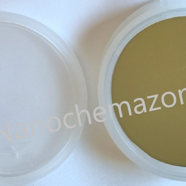
Single Crystal Silicon Wafer P-type,
Single Crystal Silicon Wafer P-type,
| Product Name | Single Crystal Silicon Wafer P-type |
| Cat No. | NCZ-NSC332/20 |
| Día | 3 inch |
| Diameter | 76.2mm ± 0.3mm (3 inches) |
| Type | P |
| Orientation | <100> |
| Thickness | 400±10um |
| Resistivity | 1-10 ohm-cm |
| Polished | Single side polished |
Description:
NanoChemazone Supplies provides both standard and customized high-quality single crystals, wafers and substrates for a wide range of applications such as LED, ferroelectric, piezoelectric, electro-optical, photonics, high power electronics, and high-frequency power devices, just to name a few. Customized crystal growth, precision machining, and coating services are available. Please contact us today to discuss your project requirements.Related Information
Please email us for the customization. Email: contact@nanochemazone.com Please contact us for customization and price inquiry Note: We supply different size ranges of Nano and micron as per the client’s requirements and also accept customization in the various parameters. Note: For pricing & ordering information, please contact us at sales@nanochemazone.com Please contact us for quotes on Larger Quantities & Customization. E-mail: contact@nanochemazone.com Customization: If you are planning to order large quantities for your industrial and academic needs, please note that customization of parameters (such as size, length, purity, functionalities, etc.) are available upon request.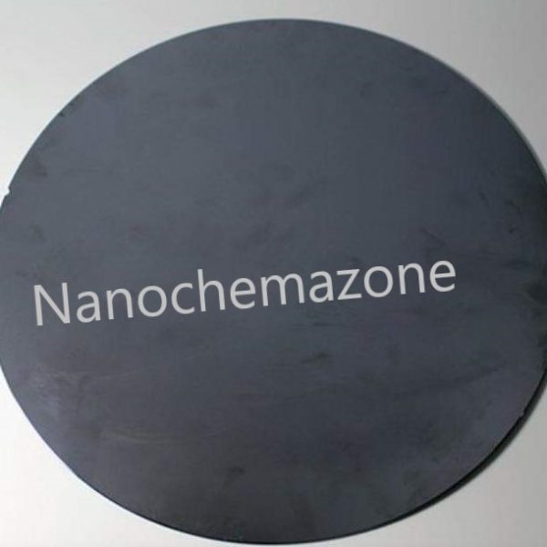
Single Crystal Silicon-Silicon dioxide Wafer
Single Crystal silicon-silicon dioxide Wafer
Product Name: Single Crystal silicon-silicon dioxide Wafer
| Product Name | Single Crystal silicon-silicon dioxide Wafer P-type (4 inches) |
| Cat No. | NCZ-NSC318/20 |
| Día | 100 mm (4 inches) |
| Orientation | <100> |
| Wafer thickness | 500 micrometer |
| Resistivity | <0.01 |
| Polished | Front Side Polished |
| Thickness | 300 nm (dry) |
| Purity | 99.9% |
| Formula | Si/SiO2 |
Single Crystal silicon-silicon dioxide Wafer P-type Description :
Provided in a single wafer caseSilicon oxide wafer SIO2 thin-film among semiconductor technology, SiO2 thin film layers are mainly used as dielectric material and more recently, they are integrated with MEMS (Micro Electro Mechanical Systems) devices. The simplest way to produce silicon oxide layers on silicon wafers is to oxidize silicon with oxygen.
Single Crystal silicon-silicon dioxide Wafer RELATED INFORMATION Storage Conditions: Airtight sealed, avoid light and keep dry at room temperature. Please email us for the customization. Email: contact@nanochemazone.com Note: We supply different size ranges of nano and micron size powder as per the client’s requirements and also accept customization in various parameters.
Reviews
There are no reviews yet.