
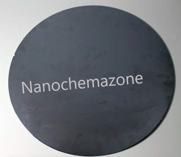
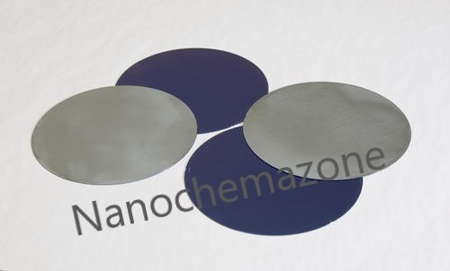
Single Crystal Silicon-Silicon dioxide Wafer
₹0.00
Single Crystal silicon-silicon dioxide Wafer
Product Name: Single Crystal silicon-silicon dioxide Wafer
| Product Name | Single Crystal silicon-silicon dioxide Wafer P-type (4 inches) |
| Cat No. | NCZ-NSC318/20 |
| Día | 100 mm (4 inches) |
| Orientation | <100> |
| Wafer thickness | 500 micrometer |
| Resistivity | <0.01 |
| Polished | Front Side Polished |
| Thickness | 300 nm (dry) |
| Purity | 99.9% |
| Formula | Si/SiO2 |
Single Crystal silicon-silicon dioxide Wafer P-type Description :
Provided in a single wafer case
Silicon oxide wafer SIO2 thin-film among semiconductor technology, SiO2 thin film layers are mainly used as dielectric material and more recently, they are integrated with MEMS (Micro Electro Mechanical Systems) devices. The simplest way to produce silicon oxide layers on silicon wafers is to oxidize silicon with oxygen.
Single Crystal silicon-silicon dioxide Wafer RELATED INFORMATION
Storage Conditions:
Airtight sealed, avoid light and keep dry at room temperature.
Please email us for the customization.
Email: contact@nanochemazone.com
Note: We supply different size ranges of nano and micron size powder as per the client’s requirements and also accept customization in various parameters.
Note: For pricing & ordering information, please contact us at sales@nanochemazone.com
Please contact us for quotes on Larger Quantities & Customization. E-mail: contact@nanochemazone.com
Customization:
If you are planning to order large quantities for your industrial and academic needs, please note that customization of parameters (such as size, length, purity, functionalities, etc.) are available upon request.
You must be logged in to post a review.
Related products

Antimony Tin oxide Powder
Antimony Tin oxide Powder
Product Name: Antimony Tin oxide powder| Product | Antimony Tin oxide powder |
| Colour | White |
| Purity | ≥ 99.9% |
| Particle size | 1-10 µM (customizable) |
| Ingredient/MF | SnO2, Sb2O3 |
| Product Code | NCZ-CM-176/20 |
| CAS Number | 18282-10-5/1309-64-4 |
- ATO has excellent electrical and optical properties that are widely used as good electrical conductivity, also as an antistatic agent widely used in paint, chemical fiber, polymer film field.
- ATO has good insulation properties. Used the ATO coating to be made of automotive glass is an excellent effect of shielding and reflecting infrared radiation.
- ATO with super fine conductive properties can be used in paints, textiles, plastics, and other fields, the direct mixing of liquid and configuration system, good compatibility.
- ATO has excellent electrical and optical properties. Used as an antistatic agent is widely used in paint, chemical fiber, polymer film field.

Bismuth Metal Polycrystalline Powder
Product Name: Bismuth Metal Polycrystalline Powder
| Product | polycrystalline |
| CAS No. | 7440-69-9 |
| Appearance | brown Powder |
| Purity | 99.9% |
| APS | 1 – 5 Microns (Can be customized) |
| Ingredient | Bi |
| Product Code | NCZ-NSC-275/20 |

D3O 10 mm Solid Sheet 10″x14.5″ (AERO) Unskived
D3O Sheets
D3O Sheets Also available in 2mm, 4mm, and 6mm Thickness.D3O Sheets with shock-absorbing properties
D3O® uses patented, patent-pending, and proprietary technologies to make rate-sensitive, soft, flexible materials with shock-absorbing properties.D3O Sheets D3O® foam sheets can be cut to size and applied to the body as an under-wrap to provide added protection to select body parts or to contusions without leaving the field for more than a few seconds. D3O® foam is soft and flexible and can be cut to any shape to match your specific needs.
Add D3O®’s patented impact protection to existing equipment by cutting your own padding. D3O® foams are made from cutting-edge smart molecules that remain soft and flexible until a force is applied causing the material to react on the molecular level by seizing up and binding together providing uncompromising impact protection.
D3O® set solid and mesh sheets reduce up to three times as much force as similar foam padding without the added bulk. Only 4mm of solid D3O® AERO out preforms 20mm of EVA foam in transmitted force testing by up to 60%. More than doubling the protective layer 10mm unskived AERO sheets are the ultimate side-line wrap.
To learn more about D3O® foam sheets and to get a glimpse at the raw testing data click the link below.
D3O-solid-mesh-sheet Pure Platinum Metal Sheet/Foil
Gallium Nitride Powder
Product Name: Gallium Nitride Powder
| Product | Gallium Nitride |
| CAS No. | 25617-97-4 |
| Appearance | Yellow Powder |
| Purity | 99.9% |
| APS | 1 – 5 Microns (Can be customized) |
| Ingredient | GaN |
| Product Code | NCZ-NSC-135/20 |
Nickel Silicide Powder
Nickel Silicide Powder
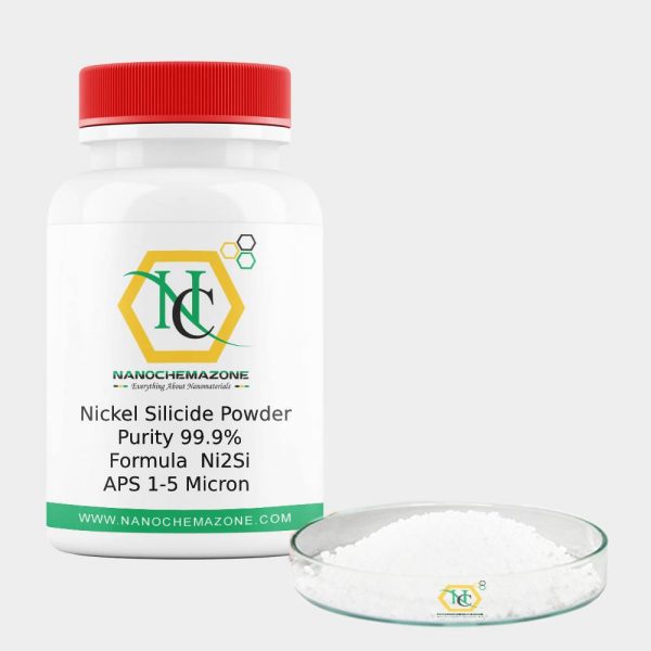
Product Name: Nickel Silicide Powder
| Product | Nickel Silicide Powder |
| CAS No | 12059-14-2 |
| Appearance | White Powder |
| Purity | 99.9% |
| APS | 1 – 5 Microns (Can be customized) |
| Ingredient | Ni2Si |
| Product Code | NCZ-NSC-133/20 |
Nickel Silicide Powder Related Information:
Nickel Silicide Powder: The reaction between SiC with chemically plated nickel on its surface has been investigated. X-ray analysis gave a good number of lattice parameters for Ni 3Si, a = 0.3522nm, and has good agreement with the index. The surface layer of Ni diffuses into the SiC and exothermically forms Ni 3Si in a defined temperature range, producing free carbon which could be deleterious to the properties.
A reaction is evident at temperatures 900°C and 1350°C with an increasing trend. The mechanism of sintering which is shown to be a reaction sintered transient-liquid phase method was determined by thermal analysis and metallographic techniques. The strength, hardness, and density properties of sintered Ni /Al (Liquid) + SiC composites are also reported.
Storage Conditions: Airtight sealed, avoid light and keep dry at room temperature. Please email us for the customization. Email: contact@nanochemazone.com Note: We supply different size ranges of nano and micron size powder as per the client’s requirements and also accept customization in various parameters.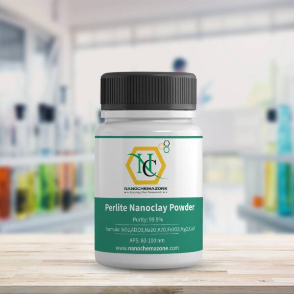
Perlite Nanoclay Powder
Perlite Nanoclay Powder
Product Name: Perlite Nanoclay Powder (Purity: > 99.9%, APS: 80-100 nm)
Product |
Perlite Nanoclay Powder |
| Cat No | NCZ-MN-142/20 |
| CAS No | 1332-58-7 |
| Purity | 99.9% |
| APS | 80-100 nm |
| Color | Gray/ off white |
| Specific Gravity | 2.2-2.4 |
| Melting Point | >2000 °F |
| pH | Neutral |
| MOHS Hardness | 5.5 |
| Water Absorption | 200-600 % by weight |
| Oil Adsorption | 50-100 grms |
| Softening Point | 1800 F or 980 |
| G.E. Brightness % | 70-80% |
| Apparent Density | 2.5-10.5 lb/ft3 |
| Wet Density | 5-20 lb/ft3 |
| Refractive Index | 1.47 |
Perlite Nanoclay Related Information
Storage Conditions: Airtight sealed, avoid light and keep dry at room temperature. Please contact us for customization and price inquiry Email: contact@nanochemazone.com Note: We supply different size ranges of Nano and micron as per the client’s requirements and also accept customization in various parameters.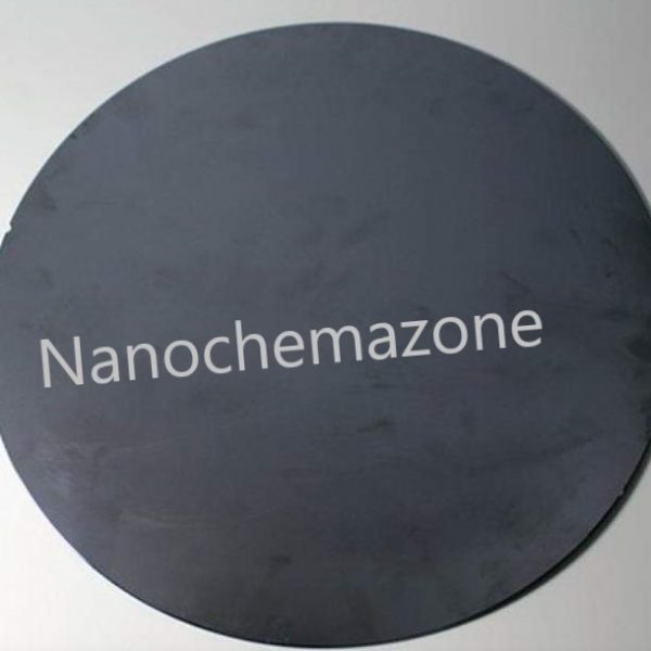
Single Crystal Silicon Wafer N-Type (3-inch)
Single Crystal Silicon Wafer N-Type (3-inch)
Product Name: Single Crystal Silicon Wafer N-Type (3-inch)
| Product Name | Single Crystal Silicon Wafer N-Type (3-inch) |
| Cat No. | NCZ-NSC333/20 |
| Type | N |
| Dia | 3 Inch |
| Doping | N-type |
| Resistivity | (1-10 Ohm/sq). |
| Thickness | 290 + 10 µm |
| Orientation | 100 |
| Polished | Single side polished |
| Form | crystalline (cubic (a = 5.4037) |
| Polished | wafer (single side polished) |
| does not contain | dopant |
| Día | 2 inch |
| Thickness | 0.5 mm |
| Boling Point | 2355 °C (lit.) |
| Melting Point | 1410 °C (lit.) |
| Density | 2.33 g/mL at 25 °C (lit.) |
| Semiconductor properties | <100>, N-type |
| SMILES string | [Si] |
Single Crystal Silicon Wafer N-Type (3-inch), NanoChemazone Supplies provides both standard and customized high-quality single crystals, wafers and substrates for a wide range of applications such as LED, ferroelectric, piezoelectric, electro-optical, photonics, high power electronics, and high-frequency power devices, just to name a few. Customized crystal growth, precision machining, and coating services are available. Please contact us today to discuss your project requirements.
Please email us for the customization. Email: contact@nanochemazone.com Please contact us for customization and price inquiry Note: We supply different size ranges of Nano and micron as per the client’s requirements and also accept customization in the various parameters.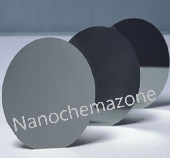
Single Crystal Silicon Wafer N-type (4-inch)
Single Crystal Silicon Wafer N-type (4-inch)
Product Name: Single Crystal Silicon Wafer N-type (4-inch)
| Product Name | Single Crystal Silicon Wafer N-type (4-inch) |
| Cat No. | NCZ-NSC331/20 |
| Día | 4 inches |
| Type | N |
| Diameter (mm) | 4” (100.8mm) |
| Type | N-Type |
| Doping | Phosphorous |
| Crystal Orientation | <100> |
| Surface: | Single Side Polished |
| Thickness | 250-500μm |
| Resistivity | 1-10ohm-cm |
| Crystal method | CZ |
| RRG (%) | ≤12 |
| Oxygen Contents (ppm) | 12.5-16.5 |
| Carbon Contents (ppm) | ≤1 |
Wafer resizing is sometimes referred to as wafer coring, re-sizing, cut down, cut-down, downsizing, down-sizing, size reducing or size reduction. We can accept orders ranging from a single wafer to hundreds of wafers per month. Our process is efficient, innovative, and ESD friendly. Our proprietary process causes less stress to the silicon wafer than other resizing methods. We also round wafer edges to eliminate edge chipping.
We frequently work with 2” (50 mm), 3” (75 mm), 100 mm (4”), 125 mm (5”), 150 mm (6”), 200 mm (8”), and 300 mm wafers; however, we are also capable of producing custom non-standard sizes.
Please email us for the customization. Email: contact@nanochemazone.com Please contact us for customization and price inquiry Note: We supply different size ranges of Nano and micron as per the client’s requirements and also accept customization in the various parameters.
Reviews
There are no reviews yet.