
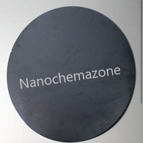
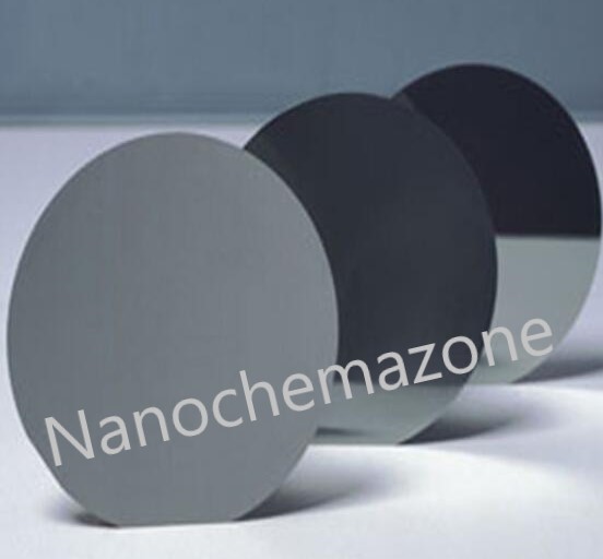
Single Crystal Silicon-Silicon dioxide Wafer
₹0.00
Single Crystal silicon-silicon dioxide Wafer
Product Name: Single Crystal silicon-silicon dioxide Wafer
| Product Name | Single Crystal silicon-silicon dioxide Wafer P-type (4 inches) |
| Cat No. | NCZ-NSC318/20 |
| Día | 100 mm (4 inches) |
| Orientation | <100> |
| Wafer thickness | 500 micrometer |
| Resistivity | <0.01 |
| Polished | Front Side Polished |
| Thickness | 300 nm (dry) |
| Purity | 99.9% |
| Formula | Si/SiO2 |
Single Crystal silicon-silicon dioxide Wafer P-type Description :
Provided in a single wafer case
Silicon oxide wafer SIO2 thin-film among semiconductor technology, SiO2 thin film layers are mainly used as dielectric material and more recently, they are integrated with MEMS (Micro Electro Mechanical Systems) devices. The simplest way to produce silicon oxide layers on silicon wafers is to oxidize silicon with oxygen.
Single Crystal silicon-silicon dioxide Wafer RELATED INFORMATION
Storage Conditions:
Airtight sealed, avoid light and keep dry at room temperature.
Please email us for the customization.
Email: contact@nanochemazone.com
Note: We supply different size ranges of nano and micron size powder as per the client’s requirements and also accept customization in various parameters.
Note: For pricing & ordering information, please contact us at sales@nanochemazone.com
Please contact us for quotes on Larger Quantities & Customization. E-mail: contact@nanochemazone.com
Customization:
If you are planning to order large quantities for your industrial and academic needs, please note that customization of parameters (such as size, length, purity, functionalities, etc.) are available upon request.
You must be logged in to post a review.
Related products

Calcium Magnesium Silicate
Calcium Magnesium Silicate
| Product |
Calcium Magnesium Silicate |
| CAS No. | N/A |
| Appearance | White |
| Purity | 99% |
| APS | 1-5µM (Can be customized) |
| Ingredient | CaMgSi2O6:Eu(2+) |
| Product Code | NCZ-NSC614/20 |
| Molecular Weight | 156.47 g/mol |
| Density | 2.9 g/cm3 |
| Melting Point | 2,130 °C (3,870 °F; 2,400 K) |
Calcium Magnesium Silicate Description
Calcium Chromate is generally immediately available in most volumes. Hydrate or anhydrous forms may be purchased. High purity, submicron and nanopowder forms may be considered. Nanochemazone produces to many standard grades when applicable, including Mil Spec (military grade); ACS, Reagent and Technical Grade; Food, Agricultural and Pharmaceutical Grade; Optical Grade, USP and EP/BP (European Pharmacopoeia/British Pharmacopoeia) and follows applicable ASTM testing standards. Typical and custom packaging is available. Additional technical, research and safety (MSDS) information is available as is a Reference Calculator for converting relevant units of measurement.
Related Information
Storage Conditions:
Airtight sealed, avoid light and keep dry at room temperature.
Please contact us for customization and price inquiry
Email: contact@nanochemazone.com
Note: We supply different size ranges of Nano and micron as per the client’s requirements and also accept customization in various parameters.
Iron Magnesium Zinc Oxide
Iron Magnesium Zinc Oxide
Product |
Iron Magnesium Zinc Oxide |
| Colour | N/A |
| Purity | 99% |
| Particle Size | 1-5µM (Customizable) |
| Ingredient/MF | MgxZn1-xFe2O4 |
| Product Code | NCZ-CP-367/20 |
| CAS Number | 15552-14-4 |
| Density | N/A |
| Melting point | N/A |
| Boiling Point | N/A |
| Molecular Weight | N/A |
| Exact Mass | N/A |
Iron Magnesium Zinc Oxide Description
Magnesium is a Block S, Group 2, Period 3 element with an atomic mass of 24.3050. The number of electrons in each of Magnesium's shells is [2, 8, 2] and its electron configuration is [Ne] 3s2. The magnesium atom has a radius of 160 pm and a Van der Waals radius of 173 pm.
Magnesium was discovered by Joseph Black in 1775 and first isolated by Sir Humphrey Davy in 1808. Magnesium is the eighth most abundant element in the earth's crust and the fourth most common element in the earth as a whole.
In its elemental form, magnesium has a shiny grey metallic appearance and is an extremely reactive. It is can be found in minerals such as brucite, carnallite, dolomite, magnesite, olivine and talc. Commercially, magnesium is primarily used in the creation of strong and lightweight aluminum-magnesium alloys, which have numerous advantages in industrial applications. The name "Magnesium" originates from a Greek district in Thessaly called Magnesia.
Iron:
Iron is a Block D, Group 8, Period 4 element with an atomic weight of 55.845. The number of electrons in each of Iron's shells is 2, 8, 14, 2 and its electron configuration is [Ar] 3d6 4s2. The iron atom has a radius of 126 pm and a Van der Waals radius of 194 pm. Iron was discovered by humans before 5000 BC. In its elemental form, iron has a lustrous grayish metallic appearance. Iron is the fourth most common element in the Earth's crust and the most common element by mass forming the earth as a whole.
Iron is rarely found as a free element, since it tends to oxidize easily; it is usually found in minerals such as magnetite, hematite, goethite, limonite, or siderite. Though pure iron is typically soft, the addition of carbon creates the alloy known as steel, which is significantly stronger.
Zinc:
Zinc is a Block D, Group 12, Period 4 element with an atomic weight of 65.38. The number of electrons in each of zinc's shells is 2, 8, 18, 2, and its electron configuration is [Ar] 3d10 4s2. The zinc atom has a radius of 134 pm and a Van der Waals radius of 210 pm. Zinc was discovered by Indian metallurgists prior to 1000 BC and first recognized as a unique element by Rasaratna Samuccaya in 800. Zinc was first isolated by Andreas Marggraf in 1746. In its elemental form, zinc has a silver-gray appearance.
It is brittle at ordinary temperatures but malleable at 100 °C to 150 °C. It is a fair conductor of electricity, and burns in air at high red producing white clouds of the oxide. Zinc is mined from sulfidic ore deposits. It is the 24th most abundant element in the earth's crust and the fourth most common metal in use (after iron, aluminum, and copper). The name zinc originates from the German word "zin," meaning tin.
Related Information
Please email us for the customization.
Email: contact@nanochemazone.com
Please contact us for customization and price inquiry
Note: We supply different size ranges of Nano and micron as per the client’s requirements and also accept customization in various parameters.
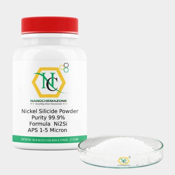
Nickel Silicide Powder
Nickel Silicide Powder
Product Name: Nickel Silicide Powder
| Product | Nickel Silicide Powder |
| CAS No | 12059-14-2 |
| Appearance | White Powder |
| Purity | 99.9% |
| APS | 1 – 5 Microns (Can be customized) |
| Ingredient | Ni2Si |
| Product Code | NCZ-NSC-133/20 |
Nickel Silicide Powder Related Information:
Nickel Silicide Powder: The reaction between SiC with chemically plated nickel on its surface has been investigated. X-ray analysis gave a good number of lattice parameters for Ni 3Si, a = 0.3522nm, and has good agreement with the index. The surface layer of Ni diffuses into the SiC and exothermically forms Ni 3Si in a defined temperature range, producing free carbon which could be deleterious to the properties.
A reaction is evident at temperatures 900°C and 1350°C with an increasing trend. The mechanism of sintering which is shown to be a reaction sintered transient-liquid phase method was determined by thermal analysis and metallographic techniques. The strength, hardness, and density properties of sintered Ni /Al (Liquid) + SiC composites are also reported.
Storage Conditions:
Airtight sealed, avoid light and keep dry at room temperature.
Please email us for the customization.
Email: contact@nanochemazone.com
Note: We supply different size ranges of nano and micron size powder as per the client’s requirements and also accept customization in various parameters.
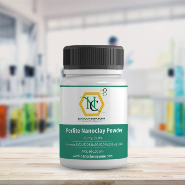
Perlite Nanoclay Powder
Perlite Nanoclay Powder
Product Name: Perlite Nanoclay Powder (Purity: > 99.9%, APS: 80-100 nm)
Product |
Perlite Nanoclay Powder |
| Cat No | NCZ-MN-142/20 |
| CAS No | 1332-58-7 |
| Purity | 99.9% |
| APS | 80-100 nm |
| Color | Gray/ off white |
| Specific Gravity | 2.2-2.4 |
| Melting Point | >2000 °F |
| pH | Neutral |
| MOHS Hardness | 5.5 |
| Water Absorption | 200-600 % by weight |
| Oil Adsorption | 50-100 grms |
| Softening Point | 1800 F or 980 |
| G.E. Brightness % | 70-80% |
| Apparent Density | 2.5-10.5 lb/ft3 |
| Wet Density | 5-20 lb/ft3 |
| Refractive Index | 1.47 |
Perlite Nanoclay Related Information
Storage Conditions:
Airtight sealed, avoid light and keep dry at room temperature.
Please contact us for customization and price inquiry
Email: contact@nanochemazone.com
Note: We supply different size ranges of Nano and micron as per the client’s requirements and also accept customization in various parameters.
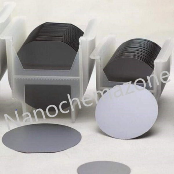
Single Crystal Silicon Wafer Diameter Intrinsic (4-inch)
Single Crystal Silicon Wafer Diameter Intrinsic (4-inch)
Product Name: Single Crystal Silicon Wafer Diameter Intrinsic (4-inch)
| Product Name | Single Crystal Silicon Wafer |
| Cat No. | NCZ-NSC327/20 |
| Diameter | 4 inches |
| Doping | undoped |
| Thickness | 400~415+/-10um |
| Resistivity | 4000 5000 ohms.cm Undoped |
| Orientation | <100>+/-0.5 |
| Polishing | one side polished |
| Application | Research Material |
| Thickness | 525 Micron |
| Resistivity | 1-10 ohm-cm |
| Polished | Single side polished |
Provided in Single wafer case.
Description:
Single Crystal Silicon Wafer thickness Is determined by the mechanical strength of the material used the wafer must be thick enough to support its own weight without cracking during handling. Wafers are grown from crystal having a regular crystal structure, with silicon having a diamond cubic structure. Orientation is defined by the Miller index with (100) or (111) faces being the most common for silicon. Ion implantation depends on the wafer’s crystal orientation since each direction offers distinct paths the transport.
Note: SSP = Single Side Polished, DSP = Double Side Polished, E = Etched, C = AsCut, Material - CZ unless noted, L = Lapped, Und = Undoped (Intrinsic)
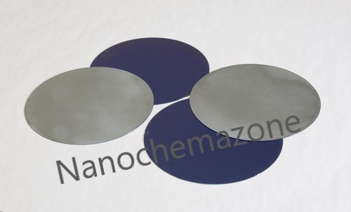
Single crystal silicon wafer Intrinsic (2-inch)
Single crystal silicon wafer Intrinsic (2-inch)
Product Name: Single crystal silicon wafer Intrinsic (2-inch)
| Product Name | Single crystal silicon wafer Intrinsic (2-inch) |
| Cat No. | NCZ-NSC329/20 |
| Diameter | 2 inch |
| Doping | Intrinsic |
| Resistivity | (>1000ohm/sq.) |
| Thickness | 400µm |
| Orientation | 100 |
| Polished | Single side polished |
Provided in a Single wafer case:
Description:
Single crystal silicon wafer Intrinsic (2-inch) is the most widely used semiconductor material as a substrate material due to its excellent machinability, mechanical stability, and the potential to combine sensing elements and electronics on the same substrate. Circular wafers made of silicon are used as a substrate in most MEMS sensors.
The crystal orientation should be known before manufacturing since silicon has orientation-dependent properties such as piezoresistivity coefficients and etching rates. The common orientation is (100) where the numbers represent Miller indices.
As an example, (100) wafer that has a primary flat side as an indication of < 110 > direction. When a piezoresistive element is placed on a (100) wafer, the orientation should be parallel to < 110 > direction if the piezoresistivity coefficients in that direction are intended to be utilized.
Please email us for the customization.
Email: contact@nanochemazone.com
Please contact us for customization and price inquiry
Note: We supply different size ranges of Nano and micron as per the client’s requirements and also accept customization in the various parameters.
Single Crystal Silicon Wafer P Type 2 Inch
Single Crystal Silicon Wafer P Type 2 Inch
Product Name: Single Crystal Silicon Wafer P Type 2 Inch
| Product Name | Single Crystal Silicon Wafer P Type 2 Inch |
| Cat No. | NZC-NSC331/20 |
| Diameter | 2 inch
|
| Doping | P-type |
| Resistivity | (1-50 Ohm/sq.) |
| Thickness | 280 + 25 µm |
| Orientation | 100 |
| Polished | Single side polished |
Provided in a single wafer case
Single crystal silicon wafer P-Type (2 inches) Description:
NanoChemazone Supplies provides both standard and customized high-quality single crystals, wafers and substrates for a wide range of applications such as LED, ferroelectric, piezoelectric, electro-optical, photonics, high power electronics, and high-frequency power devices, just to name a few. Customized crystal growth, precision machining, and coating services are available. Please contact us today to discuss your project requirements.
Single crystal silicon wafer P-Type (2 inches) Related Information
Storage Conditions:
Airtight sealed, avoid light, and keep dry at room temperature.
Please contact us for customization and price inquiry
Email: contact@nanochemazone.com
Note: We supply different size ranges of Nano and micron as per the client’s requirements and Note: For pricing & ordering information, please contact us at sales@nanochemazone.com
Please contact us for quotes on Larger Quantities & Customization. E-mail: contact@nanochemazone.com
Customization:
If you are planning to order large quantities for your industrial and academic needs, please note that customization of parameters (such as size, length, purity, functionalities, etc.) are available upon request
Single Crystal Silicon Wafer P-Type (4 Inch)
Single Crystal silicon-silicon dioxide Wafer N-type (4 inch)
| Product Name | Single Crystal Silicon Wafer P-Type (4 Inch) |
| Cat No. | NZC-NSC333/20 |
| MF | Si/SiO2 |
| Día | 100mm ± 0.5mm (4 inch) |
| Type/Dopant | P
|
| Orientation | <100>
|
| Wafer thickness | 525±25um
|
| Resistivity | 1-10 ohm-cm
|
| Polished | Single side polished
|
| TTV | < 10um
|
| SiO2 Oxide Thickness | 300 nm (dry) |
Provided in single wafer box
Crystal silicon-silicon dioxide Wafer N-type (4 inches) Description
Single crystal silicon is the most widely used semiconductor material as a substrate material due to its excellent machinability, mechanical stability, and the potential to combine sensing elements and electronics on the same substrate. Circular wafers made of silicon are used as the substrate in most MEMS sensors. The crystal orientation should be known before manufacturing since silicon has orientation-dependent properties such as piezoresistivity coefficients and etching rates. The common orientation is (100) where the numbers represent Miller indices. As an example, (100) wafer that has a primary flat side as an indication of < 110 > direction. When a piezoresistive element is placed on a (100) wafer, the orientation should be parallel to < 110 > direction if the piezoresistivity coefficients in that direction are intended to be utilized.
Note: For pricing & ordering information, please contact us at sales@nanochemazone.com
Please contact us for quotes on Larger Quantities & Customization. E-mail: contact@nanochemazone.com
Customization: If you are planning to order large quantities for your industrial and academic needs, please note that customization of parameters (such as size, length, purity, functionalities, etc.) are available upon request.
Crystal Silicon dioxide Wafer N-type (4 inches) RELATED INFORMATION
Storage Conditions:
Airtight sealed, avoid light, and keep dry at room temperature.
Please contact us for customization and price inquiry
Email: contact@nanochemazone.com
Note: We supply different size ranges of Nano and micron as per the client’s requirements and also accept customization in various parameters.
Reviews
There are no reviews yet.