
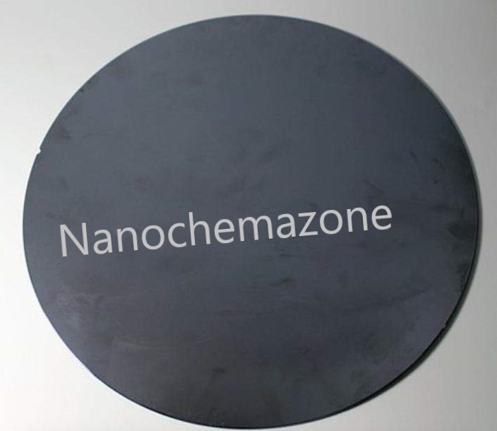
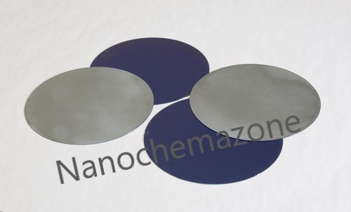
Single Crystal Silicon-Silicon dioxide Wafer
₹0.00
Single Crystal silicon-silicon dioxide Wafer
Product Name: Single Crystal silicon-silicon dioxide Wafer
| Product Name | Single Crystal silicon-silicon dioxide Wafer P-type (4 inches) |
| Cat No. | NCZ-NSC318/20 |
| Día | 100 mm (4 inches) |
| Orientation | <100> |
| Wafer thickness | 500 micrometer |
| Resistivity | <0.01 |
| Polished | Front Side Polished |
| Thickness | 300 nm (dry) |
| Purity | 99.9% |
| Formula | Si/SiO2 |
Single Crystal silicon-silicon dioxide Wafer P-type Description :
Provided in a single wafer case
Silicon oxide wafer SIO2 thin-film among semiconductor technology, SiO2 thin film layers are mainly used as dielectric material and more recently, they are integrated with MEMS (Micro Electro Mechanical Systems) devices. The simplest way to produce silicon oxide layers on silicon wafers is to oxidize silicon with oxygen.
Single Crystal silicon-silicon dioxide Wafer RELATED INFORMATION
Storage Conditions:
Airtight sealed, avoid light and keep dry at room temperature.
Please email us for the customization.
Email: contact@nanochemazone.com
Note: We supply different size ranges of nano and micron size powder as per the client’s requirements and also accept customization in various parameters.
Note: For pricing & ordering information, please contact us at sales@nanochemazone.com
Please contact us for quotes on Larger Quantities & Customization. E-mail: contact@nanochemazone.com
Customization:
If you are planning to order large quantities for your industrial and academic needs, please note that customization of parameters (such as size, length, purity, functionalities, etc.) are available upon request.
You must be logged in to post a review.
Related products

Gallium Nitride Powder
Product Name: Gallium Nitride Powder
| Product | Gallium Nitride |
| CAS No. | 25617-97-4 |
| Appearance | Yellow Powder |
| Purity | 99.9% |
| APS | 1 – 5 Microns (Can be customized) |
| Ingredient | GaN |
| Product Code | NCZ-NSC-135/20 |

Lead Telluride Powder
Product Name: Lead Telluride Powder
| Product | Lead Telluride Powder |
| CAS No. | 1314-91-6 |
| Appearance | Grey Powder |
| Purity | 99.9% |
| APS | 1 – 5 Microns (Can be customized) |
| Ingredient | PbTe |
| Product Code | NCZ-NSC-140/20 |
Lead Telluride Description :
Lead tin telluride is a ternary alloy of lead, tin, and tellurium, generally made by alloying either tin into lead telluride or lead into tin telluride. It is a narrow bandgap semiconductor material.
The bandgap is tuned by varying the composition(x) in the material. SnTe can be alloyed with Pb (or PbTe with Sn) to tune the bandgap from (SnTe). Lead Telluride Powder important to note that unlike chalcogenides, e.g. cadmium, mercury, and zinc chalcogenides, the bandgap in Te does not change linearly between the two extremes. In contrast, as the composition (x) is increased, the bandgap decreases approach zero in the concentration regime (0.32–0.65 corresponding to temperature 4-300 K, respectively) and further increases towards the bulk bandgap of SnTe. Therefore, the lead-tin telluride alloys have narrower band gaps than their endpoint counterparts making lead tin telluride an ideal candidate for mid-infrared, 3–14 μm optoelectronic application.
Lead Telluride Powder has a positive temperature coefficient i.e. for a given composition x, the bandgap increases with temperature. Therefore, temperature stability has to be maintained while working with lead-tin telluride based laser. However, the advantage is that the operating wavelength of the laser can simply be tuned by varying the operating temperature.
The optical absorption coefficient of lead-tin telluride is typical ~750 cm−1 as compared to ~50 cm−1 for the extrinsic semiconductors such as doped silicon. The higher optical coefficient value not only ensures higher sensitivity but also reduces the spacing required between individual detector elements to prevent optical cross-talk making integrated circuit technology easily.
Lead Telluride Related Information
Storage Conditions: Airtight sealed, avoid light and keep dry at room temperature. Please email us for the customization. Email: contact@nanochemazone.com Note: We supply different size ranges of nano and micron size powder as per the client’s requirements and also accept customization in various parameters.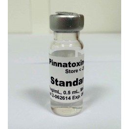
Pinnatoxin-G CAS: 1312711-74-2
Pinnatoxin-G
| Product Name | Pinnatoxin-G |
| Cat No | NCZ-000-101 |
| CAS No | 1312711-74-2 |
| Synonyms | Pinnatoxin G |
| Molecular Formula | C42H63NO7 |
| Molecular Weight | 693.95 |
Pinnatoxin-G CAS: 1312711-74-2
D3O 10 mm Solid Sheet 10″x14.5″ (AERO) Unskived
Silicon oxide wafer P-Type (2 inch)
Product Name: Silicon oxide wafer P-Type (2 inches)
| Product Name | Silicon oxide wafer P-Type (2 inches) |
| Cat. No. | NCZ-NSC318/20 |
| Diameter | 50.8+- 0.2 mm (2 inch) |
| Oxide Thickness | 300 +- 20 nm (dry) |
| Resistivity | (1-10 Ohm/sq). |
| Thickness | 300+ 15 µm |
| Orientation | <100>+- 0.5 |
Silicon oxide wafer P-Type (2 inches) Description
Provided in Single wafer caseSingle Crystal Silicon for solar energy applications includes p-type and n-type silicon. Silicon Silicon-based photovoltaic cells (PV Cells) for solar energy are fabricated from a positively charged or p-type silicon layer underneath a negatively charged or n-type silicon layer. These layers can be produced from single crystal silicon material sold under the AE Solar Energy group. Most silicon-based PV solar cells are produced from polycrystalline silicon with single-crystal systems the next most common. Silicon Metal is also available as a polycrystalline powder for casting, amorphous silicon for deposition, disc, granules, ingot, pellets, pieces, powder, rod, sputtering target, wire, and other forms and custom shapes. Ultra-high purity and high purity forms also include submicron powder and nanoscale powder. Single Crystal Silicon is generally immediately available in most volumes.
Silicon oxide wafer P-Type (2 inches) RELATED INFORMATION
Storage Conditions: Airtight sealed, avoid light, and keep dry at room temperature. Please email us for the customization. Email: contact@nanochemazone.com Note: We supply different size ranges of nano and micron size powder as per the client’s requirements and also accept customization in various parameters.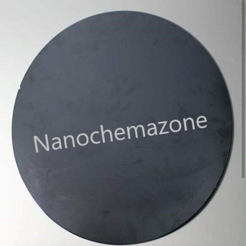
Single Crystal Silicon Wafer Diameter Intrinsic (4-inch)
Single Crystal Silicon Wafer Diameter Intrinsic (4-inch)
Product Name: Single Crystal Silicon Wafer Diameter Intrinsic (4-inch)
| Product Name | Single Crystal Silicon Wafer |
| Cat No. | NCZ-NSC327/20 |
| Diameter | 4 inches |
| Doping | undoped |
| Thickness | 400~415+/-10um |
| Resistivity | 4000 5000 ohms.cm Undoped |
| Orientation | <100>+/-0.5 |
| Polishing | one side polished |
| Application | Research Material |
| Thickness | 525 Micron |
| Resistivity | 1-10 ohm-cm |
| Polished | Single side polished |
Single Crystal Silicon Wafer thickness Is determined by the mechanical strength of the material used the wafer must be thick enough to support its own weight without cracking during handling. Wafers are grown from crystal having a regular crystal structure, with silicon having a diamond cubic structure. Orientation is defined by the Miller index with (100) or (111) faces being the most common for silicon. Ion implantation depends on the wafer’s crystal orientation since each direction offers distinct paths the transport.
Note: SSP = Single Side Polished, DSP = Double Side Polished, E = Etched, C = AsCut, Material - CZ unless noted, L = Lapped, Und = Undoped (Intrinsic)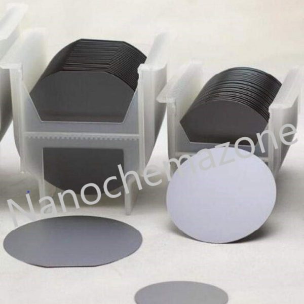
Single crystal silicon wafer N-type (2 inch)
Single crystal silicon wafer N-type (2 inch)
Product Name: Single crystal silicon wafer N-type (2 inch)
| Product Name | Single crystal silicon wafer N-type (2 inch) |
| Cat No. | NCZ-NSC332/20 |
| Diameter | 2 inch |
| Doping | N type |
| Resistivity | (1-10 Ohm/sq). |
| Thickness | 290 + 10 µm |
| Orientation | 100 |
| Polished | Single side polished |
| Form | crystalline (cubic (a = 5.4037) |
| Polished | wafer (single side polished |
| does not contain | dopant |
| dia | 2 inch |
| Thickness | 0.5 mm |
| Boling Point | 2355 °C (lit.) |
| Melting Point | 1410 °C (lit.) |
| Density | 2.33 g/mL at 25 °C (lit.) |
| Semiconductor properties | <100>, N-type |
| SMILES string | [Si] |
Single crystal silicon wafer N-type (2 inch) NanoChemazone Supplies provides both standard and customized high-quality single crystals, wafers and substrates for a wide range of applications such as LED, ferroelectric, piezoelectric, electro-optical, photonics, high power electronics, and high-frequency power devices, just to name a few. Customized crystal growth, precision machining, and coating services are available. Please contact us today to discuss your project requirements.
Please email us for the customization. Email: contact@nanochemazone.com Please contact us for customization and price inquiry Note: We supply different size ranges of Nano and micron as per the client’s requirements and also accept customization in the various parameters.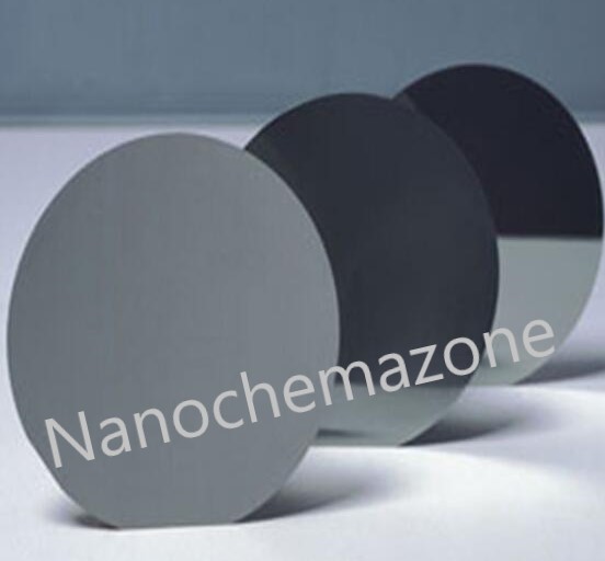
Single Crystal Silicon Wafer P-Type (4 Inch)
Single Crystal silicon-silicon dioxide Wafer N-type (4 inch)
| Product Name | Single Crystal Silicon Wafer P-Type (4 Inch) |
| Cat No. | NZC-NSC333/20 |
| MF | Si/SiO2 |
| Día | 100mm ± 0.5mm (4 inch) |
| Type/Dopant | P |
| Orientation | <100> |
| Wafer thickness | 525±25um |
| Resistivity | 1-10 ohm-cm |
| Polished | Single side polished |
| TTV | < 10um |
| SiO2 Oxide Thickness | 300 nm (dry) |
Crystal silicon-silicon dioxide Wafer N-type (4 inches) Description
Single crystal silicon is the most widely used semiconductor material as a substrate material due to its excellent machinability, mechanical stability, and the potential to combine sensing elements and electronics on the same substrate. Circular wafers made of silicon are used as the substrate in most MEMS sensors. The crystal orientation should be known before manufacturing since silicon has orientation-dependent properties such as piezoresistivity coefficients and etching rates. The common orientation is (100) where the numbers represent Miller indices. As an example, (100) wafer that has a primary flat side as an indication of < 110 > direction. When a piezoresistive element is placed on a (100) wafer, the orientation should be parallel to < 110 > direction if the piezoresistivity coefficients in that direction are intended to be utilized.
Note: For pricing & ordering information, please contact us at sales@nanochemazone.com Please contact us for quotes on Larger Quantities & Customization. E-mail: contact@nanochemazone.com Customization: If you are planning to order large quantities for your industrial and academic needs, please note that customization of parameters (such as size, length, purity, functionalities, etc.) are available upon request.Crystal Silicon dioxide Wafer N-type (4 inches) RELATED INFORMATION
Storage Conditions: Airtight sealed, avoid light, and keep dry at room temperature. Please contact us for customization and price inquiry Email: contact@nanochemazone.com Note: We supply different size ranges of Nano and micron as per the client’s requirements and also accept customization in various parameters.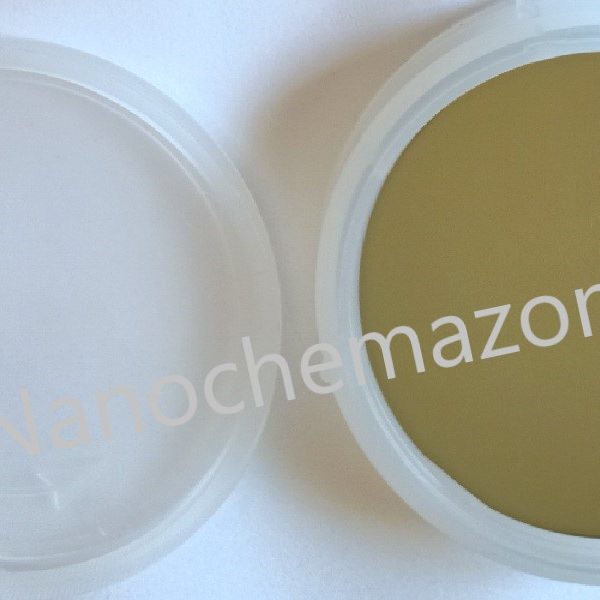
Single Crystal Silicon Wafer P-type,
Single Crystal Silicon Wafer P-type,
| Product Name | Single Crystal Silicon Wafer P-type |
| Cat No. | NCZ-NSC332/20 |
| Día | 3 inch |
| Diameter | 76.2mm ± 0.3mm (3 inches) |
| Type | P |
| Orientation | <100> |
| Thickness | 400±10um |
| Resistivity | 1-10 ohm-cm |
| Polished | Single side polished |
Reviews
There are no reviews yet.